


Let's Design and Build a (mostly) Digital Theremin!
Posted: 8/21/2016 3:35:02 PM

Panel Layout
Playing around with various rotary encoder layouts:
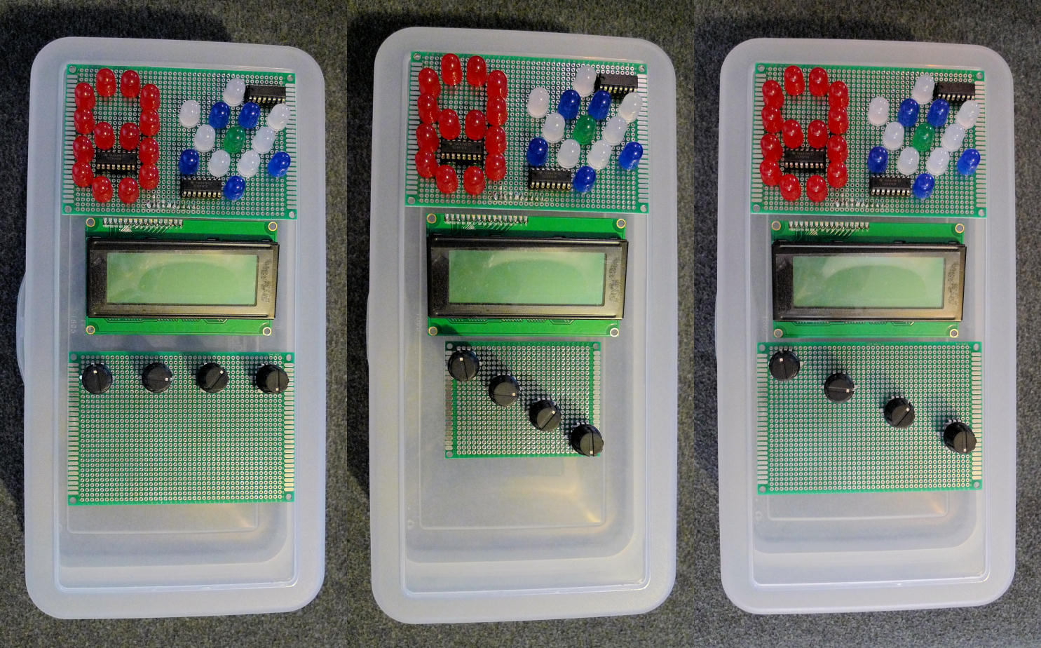
The left option is obviously the most symmetrical, so it would be best for an ambidextrous controller box, and it would also allow for the smallest physical controller box in the vertical direction. The center option appeals to me because the LCD has 4 lines, and giving the knobs some vertical association / correspondence with the LCD lines would make the interface more intuitive (I'm strongly considering having the hierarchical UI based on knob per line control) albeit less ambidextrous. The angle the knobs takes in the center option is also fairly ergonomic for a non-south-paw, allowing tight knob spacing without too much interference between the manipulation of them. The right option is a blend of the first two.
I'm struggling with which one to do because my inner cheapskate is screaming at me to do the center one so as to not to consume another LED display sized protoboard (I only have two, but I have tons of these smaller protoboards). But other parts of my brain like the other two options better and dislike the relatively cramped center one. Knobs that are too close together could be disastrous in a live performance parameter manipulation scenario, but having them close would likely speed up editing. What to do?
I could just wire the switches and pull-ups in the air, but that might be risky in terms of shorts and stuff.
[EDIT] My inner cheapskate won. Wiring it up now.
Posted: 8/23/2016 2:06:30 PM
I mounted the LED tuner, LCD module, and rotary encoder board in the prototype box yesterday (imagine the middle image above but with the stuff mounted beneath the translucent plastic top).
Today I'm doing an FPGA pin inventory and am thinking about power distribution as there are only two +5 pins, two +3.3 pins, and four ground pins on the FPGA headers. There are 80 I/O pins brought out to the FPGA board headers, and the Theremin requires somewhere around 40, so it's not a squeaker in terms of pin count. Thinking of integrating the SPI Flash, SPDIF Toslink TX, and UART interface on a small board, with multiple power and ground breakout pins. Once the pins are assigned I can move on to the oscillator interface modules at the antennas, which will mark the end of the hardware integration phase and the beginning of the serious (non-toycode) software phase.
Got a sale email from Electronic Goldmine this morning and strangely they have Toslink TX modules on sale, 25 for $5, so I rashly ordered 50 (one for every serious Thereminist in the world ;-):

I threw in a bag of 100 0.5pF-5.6pF adjustable caps for $5:

Because at some point I may try my hand at making an analog Theremin or two.
Posted: 8/27/2016 3:31:44 PM
The TOSLINK TX modules arrived today, first class USPS from Phoenix AZ in 2 days is pretty sweet. I figured they were just an LED in a box, but there is an active driver in there. 3V to 5V supply, with switching input that is easy to drive because of the buffering. It drives so easily (high impedance) you can see the LED inside lighting up with coupled 60Hz hum from your finger. Here is a datasheet:
http://www.sys-concept.com/toslink_receiver_files/Toslink-TX-Data-16Mbps-Sys.Concept.pdf
I just soldered one onto the SPI flash / power distribution board:
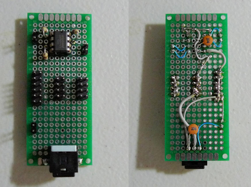
That's the SPI Flash chip at top, power distribution headers in the center (L-R: GND, 3.3V, 5V), and TOSLINK module at the bottom. The SPI Flash socket is kind of DIY, as it consists of two individual rows of socket strip (I got tired of ordering specific 14-pin, 16-pin, etc. sockets).
Posted: 8/30/2016 9:22:49 PM
The Secret 'O Life State Machines
A really weird thing about doing anything technical, but particularly coding, is how one's understanding and ability can exponentiate over time. Starting off in the hardware description biz I knew my code pretty much blew. Sure, it did what it was supposed to, but it wasn't pretty and it took me forever to write the simplest dang thing. As time went on I wrote faster and easier and better, but the distance in time I have to go back to loathe my previous work has gotten ever shorter as well. It's so bad that I find myself rewriting anything over maybe 6 months old now. I run across or develop a new technique and I want to use it everywhere it might apply, but sometimes that can have rather drastic repercussions on other aspects, so perfectly fine and functioning stuff breaks for a while, and I'm taking one step back for every two steps forward. But I'm finding and fixing bugs, so there's that. (Code review by any means necessary...)
Case in point is the RS232 UART in Hive. After FIFO buffering the LCD I decided to add FIFO buffering to the UART. But it's taken me some time to determine how to best do that. I've written many UARTs before, and have re-written this one more times than I'd like to admit (maybe 10?). What precipitated it this time is a better sense of buffering for software, and a somewhat new take on state machines. (There's also some "philosophy" of UART reception that I've acquired via much thought, but that's another story.)
As for the buffering, it makes sense to stick a FIFO between the register write side and the TX UART. You often want to kick out a bunch of digits and/or text, and don't want the processor waiting for each character to transmit. On the receive side it makes less sense to FIFO buffer, as the code is often dealing with single characters one at a time, which buffers them naturally as the algorithm goes along. Using the SPDIF 48kHz interrupt to sample the RX side leaves plenty of cushion here with 5x oversampling at 115k baud. Yes, I could software buffer the TX side as well using this interrupt, but a hardware FIFO here allows for some pretty simple toy coding. (You want simple & robust toy code.)
In terms of state machines, I've lately formed the opinion that they aren't necessarily best practice when the increase in complexity they bring doesn't pay its way. The SPDIF TX component for instance is comprised of a single up counter with various bit fields decoded for various things going on in the frame, so no formal state machine is necessary or even desired here. The LCD driver is complicated enough that it pretty much requires both counter and state machine. But the UARTs are kind of at the edge of these two spaces. My previous designs all used both counter and state machine, but I've come up with new versions that employ only counters and decode various things going on to function, and they seem easier to understand to me. Complexity always brings with it the danger of having missed something important; on the other hand you never want to do anything simple but too tricky. It's a fine line sometimes, one that I'm finally starting to dimly see.
"Believe those who seek the truth, doubt those who find it..." - André Gide
Posted: 8/31/2016 8:02:28 PM
SPI FLASH
As I did for the UARTs, I removed the state machine from my SPI Flash interface this morning, simulated it, assigned some FPGA pins to it, hooked it up to the Flash board above, and ran some experiments via the scripted terminal interface. I can read various device IDs in there, as well as read and write the Flash memory space, which is nice.
Rewriting the SPI I noticed it wasn't sampling incoming SPI data at the ideal point, so I moved the sample point to just before the SPI clock falls, where the data has had maximum time to settle but no race condition is possible. I also specified the output drive to be 4mA to give nice slow outputs and reduce ringing. The SPI clock is running at 1/4 the system clock, which I have conservatively set to 160MHz for now via one of the FPGA clock conditioning PLLs. (Top Flash speed is 50MHz for the simple read mode I'll be using.)
==============
Just remembered FPGAs usually have a "bus-hold" feature one can enable at the inputs which can help with debounce. This is equivalent to a non-inverting input buffer with a feedback resistor. The minimum drive necessary to switch a Cyclone IV input with bus-hold is 0.5 mA, which is too much for the 10k pull-up resistors I put on the encoder board. The strength of bus-hold can surprise you (in a bad way) when sprinkling what you think are "strong enough" pull-ups on your board signals.
Posted: 9/1/2016 8:59:41 PM
The Whole FPGA Shebang
Today I instantiated all of the Theremin peripherals in the FPGA (Hive core, pitch side, 2-axis volume side, tuner, LCD, rotary encoders / pushbuttons, SPDIF), assigned pinout, and worked on the timing constraints. The timing analyzer by default makes the various clock domains dependent on each other, and it takes some work to make the tool not do this. Also made it ignore any I/O timing, as everything hooked up is glacially slow compared to the FPGA logic, and inputs are resynced to the core clock where necessary. The whole shebang takes ~4k LEs (logic elements) which is ~2/3 of the device. One of the runs hit ~195MHz, though I'm holding this at 180MHz for now to keep development build times reasonable.
I don't have the LC drive / detect boards built yet, but I tested out the pitch side NCPD (numerically controlled periodic delay) for the first time and it works like a champ. Hooked the FPGA output pin directly to a 324uH coil and 10pF cap, and even out at 20ms trigger delay (max for my scope) there's only ~5ns total jitter (phase noise). Out at 20ms changing the delay value by one gives roughly 7.5ns change, which is better than 1ppm. So I'm pretty proud of my NCPD.
Posted: 9/3/2016 3:12:02 PM
Yesterday I spend a lot of time breadboarding various methods to sample the LC tank signal. I generated a square wave via the FPGA NCPD and controlled its frequency via the command line. Buffered this with a single 74LVU04N inverter, followed by a simple bipolar driver (NPN & PNP with no crossover distortion amelioration), with a fixed 10pF in place of the antenna. Its nice to finally have a signal generation source that can go significantly above 2MHz (the limit of my function generator).
I was using a capacitive divider here to knock the signal down in the past, followed by a FET or NPN follower. I found that the capacitive divider could drive a fairly low resistance (~20k ohms) without noticable phase shift, which makes sense because the capacitive reactance of a 47pF capacitor at 2.2 MHz (tank resonance) is around 1.5k ohms. So I figured I could maybe do some high / low pass filtering at this point with an RC network. Played around with topologies and values while watching the phase of the drive vs the phase and amplitude of the network output on the scope, and settled on the following, which I spiced this morning:
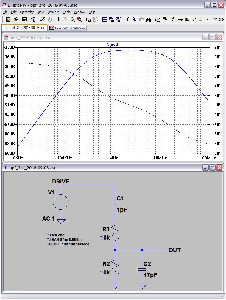
From the AC plot, we can see the attenuation is around 34dB, which is a factor of 200. We also see the phase shift is zero at the LC resonance frequency of 2.2MHz, and that the filter cutoff points (-3dB) are around 300kHz and 15MHz. The cutoff points could be moved in somewhat, but not too shabby results for just dinking around on the breadboard.
Still debating what to buffer it with, but it will likely be a transistor feeding another inverter. I feel kind of weird knocking this huge signal down and then jacking it back up again in order to measure the phase with low voltage circuitry. I wish there were some way to deal with the large signal directly and limit it somehow, it looks really pure and clean on the scope before I start messing with it.
Posted: 9/10/2016 7:57:53 PM
Generic Series LC Oscillator
Yesterday I was trying to test various tank buffering topologies in simulation, and realized that the source had to be a real (simulated) LC oscillator. So I spent several hours today designing a generic series tank LC oscillator, which pulls together a bunch of stuff I've used in the past, and some new LTSpice techniques I've just learned:
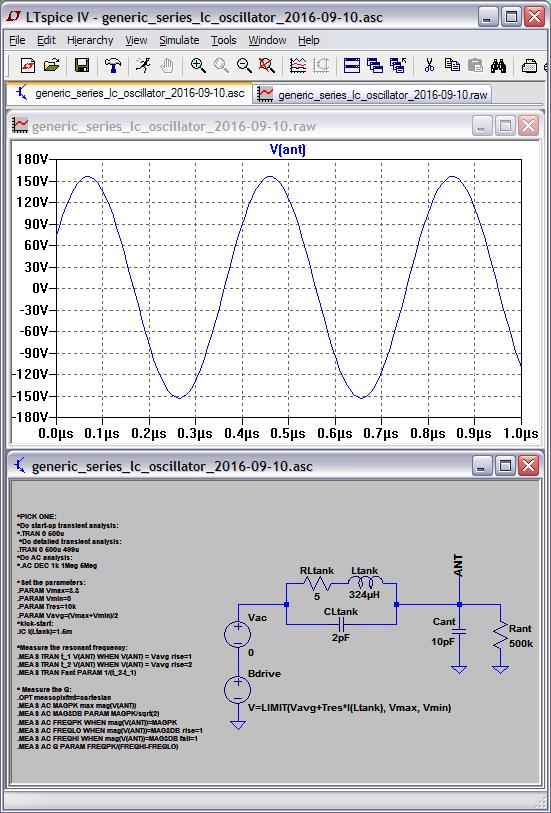
The sim uses a B source as a current controlled voltage source, where the reference current is the tank inductor current, and the output is limited using the LIMIT command. A second zero volt source is in series with it for AC analysis stimulus. You can set the min and max voltage drive values, as well as the transresistance (gain) of the B source. There are parasitics you can set for the tank inductor and antenna capacitance, and the initial "kick" (to get oscillation up and running quickly) is provided by an initial inductor current condition. Two transient simulations are provided, one from time zero to check for steady state (actual oscillation rather than just ringing from the "kick"), and a detailed end-point sim which measures the frequency of oscillation. The AC analysis measures overall Q (which is influenced up to a point by the transresistance). Measurement results may be found in the Spice error report.
Spice file here: http://www.mediafire.com/download/7cd63234dfxc5fr/generic_series_lc_oscillator_2016-09-10.asc
[EDIT] It turns out the HP/LP filter shown in the previous post is something of a Q killer (Q=26.8), so I guess it's back to a simple capacitive divider (Q=38.7). Also, I tried to use the current through Cant as the feedback, but couldn't get it to work for some reason.
Posted: 9/11/2016 9:04:11 PM
NCPD
I almost don't believe the numerically controlled periodic delay (NCPD) is working as well as it is - the math makes complete sense but it feels like my eyes are lying when I look at the scope. I have it hooked up and driving an LC tank, and the jitter anywhere I look (in terms of trigger delay, max on my scope is 50 ms if not zoomed in all the way), with every delay setting I've tried (admittedly not a ton), is seemingly constant and less than 5 ns. Since the system clock is 180 MHz, the inverse of this is 5.55 ns, which is the source of the jitter (it's dithered).
The delay control is for 1/2 of an output cycle, with two hex digits for the integer (number of system clocks) portion of the delay, and four hex digits for the fractional (sub system clock) portion of the delay. So changing the delay one least significant digit (LSD) is a delta of 1/180MHz * 1/(2^16) = 8.477 * 10^-14 ns - this is really fine control! At 50 ms trigger delay, with the LC resonating at 2.218 MHz, changing the LSD by one gives an edge location change of ~19 ns. Wow!
I guess we'll see how it behaves in a phase locked scenario, where the input numbers will change a lot, and the feedback will likely expose any weaknesses / issues. I may be able to shave some bits off of the control word (dither noise & environmental noise & feedback may make such fine control unnecessary). It's an amazing, and amazingly simple, construct. Not trying to blow my own horn nor be negative, but I'm so used to nature playing gotcha that I've come to distrust good fortune.
You must be logged in to post a reply. Please log in or register for a new account.