Let's design and build cool (but expensive) FPGA based theremin

Posted: 6/21/2019 7:43:14 PM
dewster

From: Northern NJ, USA

Joined: 2/17/2012

"Doesn't NPN based oscillator reacts on LC resonant frequency change (C change) faster than external PLL?"  - Buggins

Yes.  But above some level the rate of change is meaningless to our human senses.  And changing C in a high Q LC too quickly could perhaps kill resonance?

But when I say "phase error" I'm talking about the oscillator drive and sense not being optimally aligned.  All single transistor / logic (non PLL) oscillators I've investigated have some phase error, and this limits the voltage swing at the antenna.  The phase detector in my DPLL measures the phase difference between the drive and the antenna, and maintains it at exactly 90 degrees, giving the highest theoretical swing possible.

"Frequency of oscillator output is being measured with very high precision using ISERDES/DDR components (e.g. it's equivalent of counter with 1600MHz rate, but there can be several such meters fed with OSC signal via slightly different delays - for 8 ISERDES meters it becomes 12.8GHz).
It gives a lot of bits. E.g. if time interval between OSC edges is 1us (1MHz), single measure will give count ~ 12800. Summarized for one 48KHz sample period (~20 measurements) it gives value near 266000 (18 bits). Since OSC frequency changes only in range 6-8%, 4 higher bits do not have a meaning.
So, we have about 14 bits of oscillator frequency information collected during one sample.
Averaging will increase this value.

Does your PLL based method give more bits?"

No.  The DPLL I/O pins are DDR and driven by a 196.666MHz clock, which gives an effective sampling rate of ~400MHz, or 2 bits less than your arrangement.  I've looked into this before, and I don't believe I can use the SERDES construct in the Cyclone 4 because it is tightly integrated into the LVDS logic, which requires 2.5V bank voltage and differential I/O.  Xilinx is often a bit more basic about how things are implemented, so you can mix and match more, but sometimes that means a reduction in speed.

Since the DPLL is also driving the LC tank, everything is synchronous to the FPGA clock, which means I have to use 48kHz triangular dither to increase resolution, and to break up synchronous dead spots.  With your separate analog oscillator and very high input sample rate, I don't think you'll have that problem.

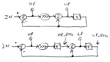
Anyway, as you know, not all bits are created equal :-).  I've got a 4th order LPF (string of 4x 1st order LPFs) for doing the hardware downsampling to 48kHz, as well as a series of notch filters in SW, and a final 4th order low-pass tracking filter that seems to effectively remove all noise.  I can see actual bit stepping changes on the LED tuner in the far field.  But I've gone a little crazy reducing all the noise I could everywhere.

It's interesting examining your register set interface.  I see you're using a moving average filter for the pitch and volume axes.  Is this for downsampling?  If so, a simple first order low-pass filter might be better suited.  A moving average weights everything the same over an interval, while low-pass weights it towards the present, otherwise they're fairly equivalent (learned this in communications class).  Moving averages can also alias more, and can require lots of memory.  My "fast" low-pass filter works up to quite high frequencies, and chaining a bunch together can give you fairly aggressive anti-aliasing.  I've got a spreadsheet on that if you're interested.  On the D-Lev I set the aggregate -3dB point to 416Hz, and the response is down -112dB at 24kHz, which gives ~18 bits of clean anti-alias action at the HW / SW interface.  Probably overkill, but at least it's blameless in terms of causing trouble.

Posted: 6/25/2019 1:37:36 PM
Buggins

From: Porto, Portugal

Joined: 3/16/2017


No.  The DPLL I/O pins are DDR and driven by a 196.666MHz clock, which gives an effective sampling rate of ~400MHz, or 2 bits less than your arrangement.  I've looked into this before, and I don't believe I can use the SERDES construct in the Cyclone 4 because it is tightly integrated into the LVDS logic, which requires 2.5V bank voltage and differential I/O.  Xilinx is often a bit more basic about how things are implemented, so you can mix and match more, but sometimes that means a reduction in speed.

So, it looks like single Xilinx Series 7 ISERDES in DDR mode (equivalent of 1.6GHz counter?) already gives more bits than 200MHz PLL (DDR->400MHz?).

If this precision exceeds noise level, adding more bits could be meaningless.

If LC oscillator gives high voltage swing on antenna (30-60V when powered by 3.3V), does it mean that phase error is low enough, and Q is high?

Sequence of 1st order IIR filters instead of moving average of course consumes less memory resources. Replacing of moving average with 1024 point FIR filter (with recent samples having bigger weight than old ones) can improve performance. Using 1 BRAM of 60 for filter doesn't look like big deal. Although, simple IIR chain may work good enough if coefficients are chosen correctly.

I'll consider redesign of averaging filter.

Posted: 6/25/2019 3:06:08 PM
dewster

From: Northern NJ, USA

Joined: 2/17/2012

"So, it looks like single Xilinx Series 7 ISERDES in DDR mode (equivalent of 1.6GHz counter?) already gives more bits than 200MHz PLL (DDR->400MHz?)."  - Buggings

Yes.

"If this precision exceeds noise level, adding more bits could be meaningless."

True in an SNR sense, though more bits can smooth over the sampling of the external oscillator (separate clock domain).

"If LC oscillator gives high voltage swing on antenna (30-60V when powered by 3.3V), does it mean that phase error is low enough, and Q is high?"

Hard to say.  FredM stated once that 50V was enough to overcome most environmental interference.  Ideally, the oscillator should support the Q of the LC tank to the best of its ability, and with air-core inductors that means hundreds of volts.  I'm not sure how to do that with analog, outside of maybe an analog PLL implementation.

"Sequence of 1st order IIR filters instead of moving average of course consumes less memory resources. Replacing of moving average with 1024 point FIR filter (with recent samples having bigger weight than old ones) can improve performance. Using 1 BRAM of 60 for filter doesn't look like big deal. Although, simple IIR chain may work good enough if coefficients are chosen correctly."

If the order is high enough you don't have to chose the coefficients very carefully at all.  My hardware 4th order uses powers of 2 (right shifts) for the coefficients and they are all identical.

What is the sampling frequency, 100MHz or so?  With 1024 FIR you get maybe 1:1000 downsampling ratio, which is 100kHz.  Don't you need that to get to 1/2 Nyquist, or 24kHz (if sampling at 48kHz)?  That was my goal anyway (anti-alias).

Posted: 6/25/2019 6:09:57 PM
Buggins

From: Porto, Portugal

Joined: 3/16/2017

If the order is high enough you don't have to chose the coefficients very carefully at all.  My hardware 4th order uses powers of 2 (right shifts) for the coefficients and they are all identical.

What is the sampling frequency, 100MHz or so?  With 1024 FIR you get maybe 1:1000 downsampling ratio, which is 100kHz.  Don't you need that to get to 1/2 Nyquist, or 24kHz (if sampling at 48kHz)?  That was my goal anyway (anti-alias).

My current implementation:

ISERDES based frequency measurement unit updates output every raising or falling edge of oscillator output. Value is time interval to previous same edge (falling - falling, or raising - raising). This value changes in 1-2 100MHz clock cycles after change occured.

Once new measure is available, it's being written to BRAM which holds 1024 or 2048 last measures.
Once per audio sample (48KHz), current position of BRAM buffer is taken as start index, then 2^N last values are being summarized (averaged). Result of summarization will be used for calculation of next sample. Actually, there may be some additional noise because OSC output may be changed at different part of sample interval. Using of higher rate for averaging filter input may prevent this. (If FIR filter is changed to faster IIR).

What is a formula of single stage of your filter?
Something like      R' = R - R>>k + V>>k 
where R' is new value of filter stage output, R is previous value, V is new input, k is filter coefficient (shift for power of 2 coefficient)?

Posted: 6/26/2019 3:22:12 PM
dewster

From: Northern NJ, USA

Joined: 2/17/2012

"Once new measure is available, it's being written to BRAM which holds 1024 or 2048 last measures.

Once per audio sample (48KHz), current position of BRAM buffer is taken as start index, then 2^N last values are being summarized (averaged). Result of summarization will be used for calculation of next sample. Actually, there may be some additional noise because OSC output may be changed at different part of sample interval. Using of higher rate for averaging filter input may prevent this. (If FIR filter is changed to faster IIR)."  - Buggins

I looked at your spice schematic for the oscillator: C=8pF, L=1.385mH, LC resonance=1.5MHz.  So this is the sampling frequency if you are sampling edge to edge.  Plugging this into my spreadsheet, the anti-alias filter could be a stage of four IIR filters operating at this frequency, all utilizing a right shift of 8.  This would give you a -3dB bandwidth of ~400Hz, with alias rejection of ~112dB at 24kHz.

The filter cutoff would track directly with the LC frequency, so as your hand approaches the antenna the filter frequency will reduce proportionally, which is the opposite of what you want, though the effect is fairly small as the LC frequency variation is rather small.

My filter is actually continuously sampling the offset triangle wave in the DPLL (accumulated phase error) at 1/2 the clock rate (~100MHz) using a right shift of 14, so the filter cutoff frequency is fixed at ~415Hz regardless of the LC resonance.  Though the DPLL forms a first order low-pass filter for phase noise, and the cutoff point of that is inversely proportional to LC frequency.  Continuous sampling gets me away from any errors associated with edge position, though I did have to examine how attenuated the filtered triangle wave becomes as it is a definite source of aliasing.

"What is a formula of single stage of your filter?
Something like      R' = R - R>>k + V>>k 
where R' is new value of filter stage output, R is previous value, V is new input, k is filter coefficient (shift for power of 2 coefficient)?"

That's the formula for a simple low-pass IIR:  R' = R + [(V - R) >> k]. 

Mine also registers the high-pass:

Code:
	// hp & lp
	always_comb hp = data_i - lp_reg;
	always_comb hp_shr = hp >>> SHR;
	always_comb lp = DATA_W'( lp_reg + hp_reg );

	// reg
	always_ff @ ( posedge clk_i or posedge rst_i ) begin
		if ( rst_i ) begin
			hp_reg <= 0;
			lp_reg <= 0;
		end else begin
			if ( en_i ) begin
				hp_reg <= hp_shr;
				lp_reg <= lp;
			end
		end
	end

	// output
	always_comb lp_o = lp_reg;

Posted: 6/26/2019 4:07:25 PM
Buggins

From: Porto, Portugal

Joined: 3/16/2017

Mine also registers the high-pass:

I dont't see difference between your code and formula.


Is there any difference between always_comb and assign?


BTW, I've checked if Xilinx Vivado supports SystemVerilog.
Found no issues so far.

Posted: 6/26/2019 6:59:14 PM
dewster

From: Northern NJ, USA

Joined: 2/17/2012

"I dont't see difference between your code and formula."  - Buggins

Here's a signal flow view:


At top is the normal high-pass / low-pass IIR, in hardware one would normally use the registered version of the LP output in order to reduce external combinatorial delays and speed things up.  At bottom is my "fast" high-pass / low-pass IIR, where the right shifted HP is registered, this time to speed things up internally.  If the cutoff frequency is low compared to the sampling frequency then these two forms have almost identical responses.  The "fast" version actually consumes the same amount of logic cells as the normal version in the Cyclone FPGA I'm using, as the registers would be orphaned otherwise.

"Is there any difference between always_comb and assign?"

No, but always_comb is safer.  I highly recommend the use of System Verilog, it's a super-set of verilog, and all of the extra features and safeties are really nice.  The .* auto-connect really cuts down on typing and typos when instantiating modules, and the packaging system is wonderful.  A single "logic" type gets you away from all that annoying "reg" and "wire" nonsense too.

Here are a couple of great papers on System Verilog:
http://www.sutherland-hdl.com/papers/2013-SNUG-SV_Synthesizable-SystemVerilog_paper.pdf
https://lcdm-eng.com/papers/snug06_Verilog%20Gotchas%20Part1.pdf

Posted: 7/2/2019 7:06:41 AM
Buggins

From: Porto, Portugal

Joined: 3/16/2017

Thank you for useful links.

My project update:

Finally got all my ordered PCBs:

Soldered two oscillator boards (sp721 ESD protection ICs are not installed, waiting for delivery).
Not yet tested.

Winded two inductors.
Frame is a 60mm length pieces of 32mm plastic water pipe.
Winding length is ~44mm
1) 0.2mm copper wire: 0.65mH  -- for pitch
2) 0.1mm copper wire: 2.3mH -- for volume
Thank you for pointing at LC meter - ordered the same device.
It's very hard to wind 0.1mm wire (spend over 4 hours for this inductor).
Will check if 0.65mH is good enough for pitch sensor. If not, I would have to wind another one with 0.1mm wire and shorter winding length.
LTSpice model of oscillator: 

Simulation results:

KiCad schematics of oscillator (pdf link)  (PCB gerber file)

Other PCBs are:

1) Main board: shield for Cora Z7 board
(gerber file link) (KiCAD schematics PDF link)

2) Encoders board: 5 encoders (with buttons) + 1 tact button - connected via only 5 pins using multiplexer (3*5 + 1 = 16 bits read using 4 pins for address and 1 pin for MUX output). Contains analog debouncing filters and pullup resistors for all 16 signals.
(gerber file link) (KiCAD schematics PDF)

3) PMod adapter connectors - just helping to place two audio PMods above shield keeping two Cora Z7 PMod ports free for future extensions.

4) Audio connectors board - for both Line In and Line Out, has big 6.3mm and small 3.5mm audio jack sockets. Wires with 3.5mm jacks on I2S2 PMod side will be soldered to this board.

5) Expression pedals interface board. Contains six 6.3mm TRS sockets for connecting of 6 expression (pot based) pedals to 6 Cora Z7 ACD inputs. sp721 is routed on shield board for protecting ADC pins from ESD. RC filters for pot output are routed for each pedal.

6) Strange PCB with 4 mounting holes and big hole inside is just for mounting WaveShare 4.3" 800x480 Touch LCD. I decided that it's better to order it from PCB manufacturer ($5 for 5 PCBs) than trying to make some mounting by myself. As a bonus, LCD mounting board contains prototyping field - just in case


Recent FPGA programming results:

Implemented in SystemVerilog debouncer with 16->1 mux input interface which provides 16 debounced bits and change flags for each bit.
Working at 100 MHz base clock. Once per 32 clocks (~3MHz), changes MUX address to next one. Checks each buttons/encoders pin state once per 100MHz/32/16 ~ 200us. 16 per-channel 10 bit counters in register bank are used to ensure input is unchanged for 100ms to avoid bouncing switches.
Once per 200us cycle, output is being updated with 16 new state values, and 16 change flags showing if value has been changed since last update or not.


Small enough resources used for 16 10-bit counters

Code:
+----------------------------+------+-------+-----------+-------+
|          Site Type        | Used | Fixed | Available | Util% |
+----------------------------+------+-------+-----------+-------+
| Slice LUTs*                |  76 |    0 |    17600 |  0.43 |
|  LUT as Logic            |  66 |    0 |    17600 |  0.38 |
|  LUT as Memory            |  10 |    0 |      6000 |  0.17 |
|    LUT as Distributed RAM |  10 |    0 |          |      |
|    LUT as Shift Register  |    0 |    0 |          |      |
| Slice Registers            |  59 |    0 |    35200 |  0.17 |
|  Register as Flip Flop    |  59 |    0 |    35200 |  0.17 |

BTW, what is reasonable debouncing time for encoders and buttons from your experience? Is 200ms ok? Hardware debouncing RC filters are present.

Posted: 7/2/2019 2:01:51 PM
dewster

From: Northern NJ, USA

Joined: 2/17/2012

"BTW, what is reasonable debouncing time for encoders and buttons from your experience? Is 200ms ok? Hardware debouncing RC filters are present."  - Buggins

I don't have RC filters on my prototype, though Roger added them to his, so I can't speak to that yet (Roger sent me a board set with RC filters but I haven't fired them up yet).  

Here is my debouncer that pre-processes each rotary encoder pin (but not the pushbuttons) (clock for all is 180MHz).   It uses a linear counter rather than IIR filter.  The debounce count range is roughly 3/4 * 2^DEB_W, and the hysteresis zone is roughly 1/3 the count range.  For example, for DEB_W = 8: count is [-97:96]; hysteresis is [-33:32].  I've found that DEB_W = 14 is sufficient (so far, encoders tend to age out):

Code:
	// resync input
	always_ff @ ( posedge clk_i or posedge rst_i ) begin
		if ( rst_i ) begin
			in_sr <= '1;
		end else begin
			in_sr <= SYNC_W'( { in_sr, data_i } );
		end
	end

	// form the up/down counter
	always_ff @ ( posedge clk_i or posedge rst_i ) begin
		if ( rst_i ) begin
			deb <= 0;
		end else begin
			if ( in_sr[SYNC_W-1] && ~max_f ) begin
				deb <= deb + 1'b1;
			end else if ( ~in_sr[SYNC_W-1] && ~min_f ) begin
				deb <= deb - 1'b1;
			end
		end
	end

	// decode flags
	always_comb max_f = ( deb[DEB_W-1EB_W-3] == 3'b011 );
	always_comb hi_f  = ( deb[DEB_W-1EB_W-3] == 3'b001 );
	always_comb lo_f  = ( deb[DEB_W-1EB_W-3] == 3'b110 );
	always_comb min_f = ( deb[DEB_W-1EB_W-3] == 3'b100 );

	// output register
	always_ff @ ( posedge clk_i or posedge rst_i ) begin
		if ( rst_i ) begin
			data_o <= 0;
		end else begin
			if ( hi_f ) begin
				data_o <= '1;
			end else if ( lo_f ) begin
				data_o <= '0;
			end
		end
	end

(The smiley face is : followed by D)  The debounced outputs are inverted, converted from Gray to binary, then fed to a simple state machine formed by a 3 bit counter.  cnt_o is incremented @ CW; decremented @ CCW, and clear on read.  Outputs are active high until read:

Code:
	// combine & invert
	always_comb enc_not = ~enc_deb;

	// convert input Gray-code to binary
	assign enc_bin = { enc_not[1], ^enc_not };

	/*
	-------------------
	-- state machine --
	-------------------
	*/

	// state mux
	always_comb begin
		if ( enc_bin == 0 ) begin
			state_sel <= 0;  // detent position
		end else begin
			state_sel <= state;  // default is stay in current state
			if ( enc_bin - state[1:0] == 2'b01 ) begin  // +1
				state_sel <= state + 1'b1;  // go clockwise
			end else if ( enc_bin - state[1:0] == 2'b11 ) begin  // -1
				state_sel <= state - 1'b1;  // go counter-clockwise
			end
		end
	end

	// register state
	always_ff @ ( posedge clk_i or posedge rst_i ) begin
		if ( rst_i ) begin
			state <= 0;  // detent position
		end else begin
			state <= state_sel;
		end
	end


	/*
	------------
	-- output --
	------------
	*/

	// output
	always_ff @ ( posedge clk_i or posedge rst_i ) begin
		if ( rst_i ) begin
			rd <= 0;
			cnt_o <= 0;
		end else begin
			rd <= rd_i;
			if (( state_sel == 0 ) && ( state == 3 )) cnt_o <= cnt_o + 1'b1;  // CW
			else if (( state_sel == 0 ) && ( state == -3 )) cnt_o <= cnt_o - 1'b1;  // CCW
			else if ( rd )	cnt_o <= 0;  // clear on read
		end
	end

This goes to the register set to be sampled and accumulated at 48kHz by the processor.  This is then sub-sampled and cleared at 12Hz to detect rotary velocity and scale the rotary change.

For the pushbuttons, I looked at them on the scope and going from closed to open doesn't bounce, and open to closed only bounces a little.  So I've found that I only need to resync them, and then store them in a clear on read register going to the processor, where I'm careful not to miss any low events:

Code:
	// register & resync
	always_ff @ ( posedge clk_i or posedge rst_i ) begin
		if ( rst_i ) begin
			rd  <= 0;
			pb_sr <= '1;
		end else begin
			rd <= rd_i;
			pb_sr <= SYNC_W'( { pb_sr, pb_i } );
		end
	end

	// latch input low (takes precedence over) clear on read
	always_ff @ ( posedge clk_i or posedge rst_i ) begin
		if ( rst_i ) begin
			pb_o  <= 0;
		end else begin
			if ( ~pb_sr[SYNC_W-1] ) begin
				pb_o <= '1;
			end else if ( rd ) begin
				pb_o <= 0;
			end
		end
	end

Then in software I sample these at 48kHz and OR them to a register (to preserve low events), and the sub-sampling and clearing of this at 12Hz surprisingly forms a natural debounce (I had to think about this for a while to understand it).

Posted: 7/8/2019 6:34:03 AM
Buggins

From: Porto, Portugal

Joined: 3/16/2017

Assembled encoders board:

Board contains 5 encoders with buttons and one button.
Mux is used to minimize number of pins needed. Without mux, 3*5+1 = 16 pins would be used.
With mux, board is connected to FPGA using 5 pins: 4 output pins for MUX address, 1 input pin for reading addressed button/encoder pin state.

Encodes module interface:

Code:
module encoders_board(
    input CLK,
    input RESET,
    
    // for reading encoders and button signals using MUX
    
    // MUX address for multiplexing N buttons into one MUX_OUT
    output logic [3:0] MUX_ADDR,
    // input value from MUX (MUX_OUT <= button[MUX_ADDR])
    input logic MUX_OUT,

    // exposing processed state as controller registers
    
    // packed state of encoders 0, 1
    // [31]    encoder1 button state
    // [30:24] encoder1 button state duration
    // [23:20] encoder1 pressed state position
    // [19:16] encoder1 normal state position
    // [15]    encoder0 button state
    // [14:8]  encoder0 button state duration
    // [7:4]   encoder0 pressed state position
    // [3:0]   encoder0 normal state position
    output logic[31:0] R0,
    // packed state of encoders 2, 3
    // [31]    encoder3 button state
    // [30:24] encoder3 button state duration
    // [23:20] encoder3 pressed state position
    // [19:16] encoder3 normal state position
    // [15]    encoder2 button state
    // [14:8]  encoder2 button state duration
    // [7:4]   encoder2 pressed state position
    // [3:0]   encoder2 normal state position
    output logic[31:0] R1,
    // packed state of encoder 4, button and last change counter
    // [31]    button state
    // [30:24] button state duration
    // [23:16] duration (in 100ms intervals) since last change of any control
    // [15]    encoder4 button state
    // [14:8]  encoder4 button state duration
    // [7:4]   encoder4 pressed state position
    // [3:0]   encoder4 normal state position
    output logic[31:0] R2
);


Input address is changed at 100MHz/32 == 3MHz frequency. All pins are checked in one 100MHz/32/16 = 200KHz clock cycle.
Debouncer uses 12 bit counter - only if input has the same value for 4096 cycles, it can switch its state.
So, minimal time for switching is 1/50 of second. Output of debouncer is 16bit of button/encoder pin states, 16 bit change flags (1 for corresponding bit if it's changed since last cycle) and UPDATE signal, which is set to 1 for one 100MHz clock cycle once per 10ms.

To minimize CPU (PS) part of driver, some useful logic has been implemented inside FPGA.

For each button, encoders module provides 8 bits: one flag (current button state) and 7 bit counter - number of 0.1s intervals since last change (can measure up to 12 seconds, stays at 127 if interval exceeds number of bits available for counter).

For each encoder, there are two 4 bit counters - one for pressed encoder button state, one for normal state.
If encoder shaft is being rotated, corresponding counter is being increased or decreased depending on rotation direction.
So, UI will be able to detect all changed even if checks board state 2-3 times per second - up to 7 rotation ticks will be remembered in counters.
If more than 7-8 ticks are made since last check, there will be overflow: e.g. 10 rotation ticks CW give the same value as 6 ticks CCW.

This design utilizes 184 LUTs (1.05%), 12 of which are used as register bank (distributed RAM 12x16).

Source code is published on GitHub

I've created page for build instructions of my design.


You must be logged in to post a reply. Please log in or register for a new account.