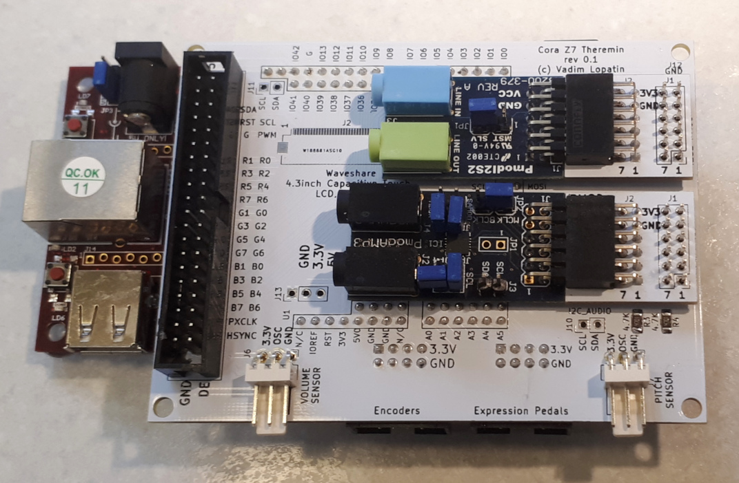
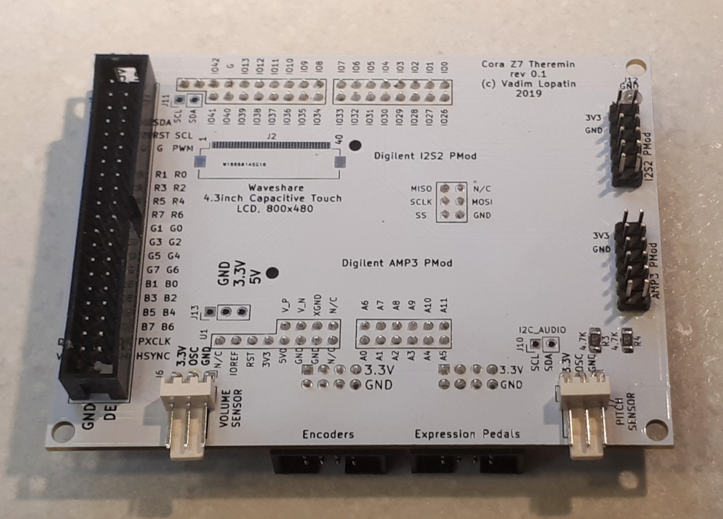
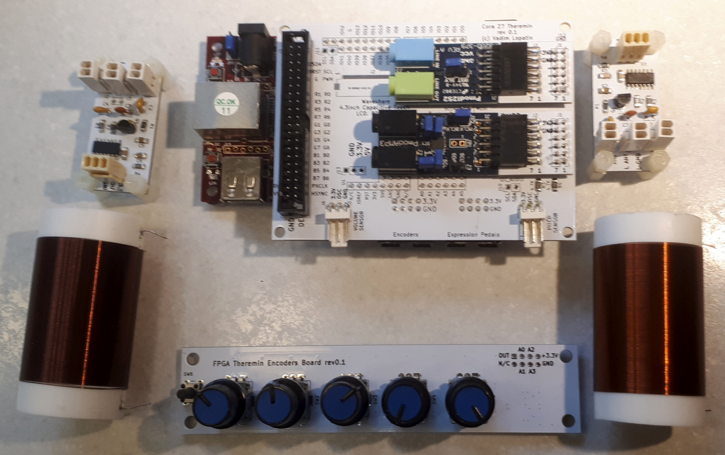
Let's design and build cool (but expensive) FPGA based theremin

Posted: 7/30/2019 12:23:27 PM
Buggins

From: Porto, Portugal

Joined: 3/16/2017

Project update:

Completely rewritten / redesigned theremin sensor module. Now it's completely in SystemVerilog.
Pitch and volume signal period measure and IIR filter.
Source code is available on GitHub

Contains Xilinx (Series7) specific resources usage.
Both Pitch and Volume frequency measure use DDR deserializer with x8 oversampling based on delay primitives.
Single channel of signal period measurement uses ISERDESE2 on 600MHz (150MHz output) deserializer working in DDR mode (gives 600MHz*2 = 1.2GHz measurement precision). Oversampling deserializer uses 8 such channels with inputs fed with original signal delayed by different delays. Output is 64 bit parallel deserialized value avalable each 150MHz cycle. Precision is equivalent of 1.2GHz * 8 = 9.6GHz counter.
Parallel 64 bits are converted to change flag and changed bit number.
On next step, flag and bit number are used to accumulate unchanged value period duration. Output is duration since last change (in 9.6GHz ticks) and change flag.
Next step: convert sequence of half-periods to periods (two recent half-periods give time interval since the same edge of signal). This is needed for proper support of non-50% duty cycle signals). As well it adds one more bit of output result.
Output of period measure gives 14-16 bits of signal (depending on source signal frequency). 

Double channel IIR filter with configurable number of stages (4 by default) and 1/2^k coefficients implements averaging and increases number of available bits. 8 bit right shift is now used as filter K.
Each 100MHz/2/4 = 12.5 MHz cycle, new value of pitch and volume IIR filter outputs is available.
Output is now configured to provide 28 bits of data.

This design in current configuration (both volume and pitch have x8 oversampling, 28 output bits) utilizes <400 LUTs (<2% of available resources).

Next steps to do in Theremin Sensor implementation:
1) Scaling - output of IIR filter should be converted to desired range (normalized) -  (value_in - min)*out_range/(max-min)
2) Linearization - non-linear input from previous stage should be converted to linear distance 
3) Distance to note, note to frequency (phase increment)
4) Distance to volume

So far, I'm unsure what is better approach - table based approximation or some program for soft core inside sensor.

If soft CPU selected for controller extension, it can replace IIR filter (which uses 100LUTs). One or two threads of CPU may work as IIR for sensor data.


Posted: 7/30/2019 2:47:49 PM
dewster

From: Northern NJ, USA

Joined: 2/17/2012

"So far, I'm unsure what is better approach - table based approximation or some program for soft core inside sensor.

If soft CPU selected for controller extension, it can replace IIR filter (which uses 100LUTs). One or two threads of CPU may work as IIR for sensor data."  - Buggins

I think it's best to get the raw data filtered to the point where you can sample it without significant aliasing at 48kHz in SW, then go from there.

Mains hum filtering is best done in SW, and the final 4th order LPF that sets the gestural bandwidth (and chops off remaining HF hum that wasn't removed via notch filtering) can be used to track the pitch hand, lowering the bandwidth in the far field where it is noisiest due to nulling (subtraction).  After filtering comes the nulling, linearization, scaling, and offsetting.  Linearization using my algorithm is really pretty trivial in SW, I imagine it could be modified to use period rather than frequency.  More importantly, it is a very easy and non-critical adjustment for the user to perform.

Is there a reason you're using 150MHz?  I'm using a multiple of 48kHz (actually a multiple of 48.014.322kHz at that's as close as I can get with a 50MHz xtal and the FPGA PLL resources).  196.666666MHz, actually.  Makes wide fast filters kinda tough to implement though. 

I really envy your input sampling resolution!  With that resolution, hum and thermal noise should be sufficient to dither things.

How are you liking SystemVerilog?  I absolutely love it, though I wish it hadn't inherited the idiotic signed/unsigned convention (i.e. gotchas) of C (if anything - and I mean anything! - is unsigned then the operation is unsigned) as it gets me every freaking time, no matter how careful I am.

Posted: 7/30/2019 5:35:59 PM
Buggins

From: Porto, Portugal

Joined: 3/16/2017

Having 48KHz multiple as processing frequency seems like good idea to avoid aliasing issues when sampling sensor data at 48000 Hz.
150MHz is just 600MHz/4. 600MHz is highest available frequency which can be used with ISERDESE2 on my low speed grade Zynq Z7-10 device used in Cora Z7.
Nice near to 150MHz limit multiply of 48000 Hz is 48000*1024*3 = 48000*3072 = 147456000
IIR filter (2 channel, 4 order, 28+8 bits of internal precision) may be optimized to support this frequency instead of currently used 100MHz. It will speed up filter cycle from 12.5MHz to 18.5MHz. Btw, more stages (up to 8th order) may be added to IIR filter at no cost (anyway, register bank - distributed ram based - has 16 registers but only 8 are used - 4 for pitch and 4 for volume).
Maybe, it makes sense to get other modules to work at this frequency to avoid cross clock domain conversions.

Cora Z7 has 120MHz clock source available for PL (and 2 PLLs) and 667 MHz CPU clock source - PLL can use several clocks generated from PS PLL.
Not sure if exact 48000 can be generated based on these frequencies.

I've tried a lot of different implementations of oversampling. In latest design, adding of x8 oversampling does not consume a lot of resources. Even Volume sensor may use the same oversampling although big sensitivity is not required for volume antenna.

I really like SystemVerilog. It has a lot of useful features. I'm just not sure if my coding style is idiomatic enough.

Posted: 7/30/2019 8:10:20 PM
dewster

From: Northern NJ, USA

Joined: 2/17/2012

"Maybe, it makes sense to get other modules to work at this frequency to avoid cross clock domain conversions."  - Buggins

Yes, I keep clock domains to an absolute minimum.  Only 2 in the D-Lev FPGA, 196.666666MHz for all the axis DPLLs and filtering, 180MHz for the processor core and peripherals.  The processor threads are all interrupted at a ~48kHz rate (derived from 196.666666MHz), and the axis DPLLs freeze the axis data they present to the processor from one interrupt to the next, in order to relax timing between the domains and keep sampling in sync.

"Not sure if exact 48000 can be generated based on these frequencies."

It doesn't have to be exact.  Mine is off by 300ppm or so, which I've read is the limit of allowable SPDIF error, but I think most SPDIF timing slaves are more tolerant than that.

Posted: 7/31/2019 2:31:52 PM
Buggins

From: Porto, Portugal

Joined: 3/16/2017

I've optimized IIR filter, now it is working at 150MHz, and utilizes only ~80 LUTs (but uses 2 DSP blocks).
Two dsp blocks are used to replace ~100 LUTs and flip-flops
Clock domain adapters are removed.

Total resources used for design: 285 (1.62%) of LUTs and 2 DSPs (2.5%). Density: 2.5% of slices are used (utilization density is 65%).

Code:
+----------------------------+------+-------+-----------+-------+
|          Site Type        | Used | Fixed | Available | Util% |
+----------------------------+------+-------+-----------+-------+
| Slice LUTs                |  285 |    0 |    17600 |  1.62 |
|  LUT as Logic             |  261 |    0 |    17600 |  1.48 |
|  LUT as Memory            |  24  |    0 |     6000 |  0.40 |
|    LUT as Distributed RAM |  24  |    0 |          |       |
|    LUT as Shift Register  |    0 |    0 |          |       |
| Slice Registers           |  352 |    0 |    35200 |  1.00 |
|  Register as Flip Flop    |  352 |    0 |    35200 |  1.00 |
|  Register as Latch        |    0 |    0 |    35200 |  0.00 |


+----------------+------+-------+-----------+-------+
|    Site Type  | Used | Fixed | Available | Util% |
+----------------+------+-------+-----------+-------+
| DSPs          |    2 |    0 |        80 |  2.50 |
|  DSP48E1 only |    2 |      |          |      |

This design measures periods of two signals with 9.6GHz precision, and filters them, providing updated outputs (28 bits) once per 8 150MHz cycles (if number of filter stages is set to 4). Filter K is fixed (module parameter), but number of stages may be changed in runtime (2-8).

Updated code is available on github.


Next step: develop barrel soft CPU core, ~150MHz clock, 4 threads (single thread effectively executed at 37MHz), 32bits, 16x16 multiplication support, 1 bit shifts

Posted: 8/5/2019 6:14:00 AM
Buggins

From: Porto, Portugal

Joined: 3/16/2017

It looks like my soldering skills are too poor for soldering of 0.5mm pitch FPC connectors.
Hopefully, IDC connection for LCD is available as well.
MicroSD socket is hard to solder, too.
SMD 1206 and SOIC are ok.

Posted: 8/6/2019 10:44:58 AM
Buggins

From: Porto, Portugal

Joined: 3/16/2017

Cora Z7 Theremin Shield PCB is assembled.

Top view:

Bottom view:

All components of design which are ready:

Page with theremin shield PCB design description is created on github.

Posted: 8/6/2019 8:41:19 PM
dewster

From: Northern NJ, USA

Joined: 2/17/2012

I like the white PCB motif!  And your coils are beautiful!

Posted: 8/7/2019 5:06:12 AM
Buggins

From: Porto, Portugal

Joined: 3/16/2017


I like the white PCB motif!  And your coils are beautiful!


Plastic box I'm going to use as prototyping cabinet has transparent top. Coils and PCBs will be visible. I hope it will look cool.

Posted: 8/8/2019 2:12:58 PM
Buggins

From: Porto, Portugal

Joined: 3/16/2017

LCD controller is rewritten from scratch in SystemVerilog (source code on github).
Trying to minimize FPGA resource usage.

16bit color, 800x480 pixels implementation with framebuffer accessed via 32-bit DMA with FIFO (via AXI3 interface) and RGB interface output takes 123 LUTs (0.7%) and half of BRAM module (0.83%).
Includes 8-bit PWM for backlight control.
Frame start address is set as a parameter (when 0, display is disabled).
DMA interface clock: ~150MHz
Pixel clock: 36.8MHz
Refresh rate: 93Hz

Two writeable registers: 
   frame start address
   backlight brightness
One readonly register:
   current row

Current row may be used to track current display position or VBlank to change buffer content while it's not being displayed.

In future, I'll add hardware support for displaying current note highlight and tuner output. Since only 12 bits of color are supported in my PCB, unused 4 bits will be used to indicate special kind of pixel data which should be processed in hardware.

Nearest plans: implement everything needed for simple working theremin with most of functions done on CPU side.

FPGA part:
Implement audio (I2S) controller (2 stereo outputs, 1 input) with sample interrupt to CPU (once per 48000Hz).
Implement ADC controller (read and filter 6 ADC inputs from analog pedals)
Implement double channel I2C (one for LCD touch controller access, one for Phones volume control)
Pack everything into single AXI4 peripherial accessible from CPU side
Add drivers for all peripherials (.h file with list of registers)
Make block design 

Hardware:
Solder audio connectors board
Solder pedal connectors board
Make IDC cables
Finish building prototype

CPU part:
Implement minimal working software to use theremin with some simple synthesizer.

You must be logged in to post a reply. Please log in or register for a new account.