Let's design and build cool (but expensive) FPGA based theremin

Posted: 6/4/2021 1:47:23 PM
Buggins

From: Porto, Portugal

Joined: 3/16/2017


Ah, in that case the D-Lev LCDPLL is soft (LUT+FF) and not a special PLL hardware block in the FPGA.
-- dewster

I was sure that you are using some hardware block. So, PLL I'm developing will be close to your one.

I use the DDR element at I/O.  With core clock of 180MHz this gives 360MHz effective resolution,
which is sufficient - but you always want everything you can get here, and if I had your 8x serdes I'd be using it for sure.
-- dewster

Then I can be sure that 1.2GHz resolution should be enough.


Tried to search altera docs for SERDES hardware blocks.

LVDS SERDES (ALTLVDS) docs say:


Code:
Turn off this option to use the dedicated SERDES circuitry in
the device. When you implement the dedicated SERDES in
the LVDS transmitter, the SERDES connects to the LVDS
transmitter; therefore, the output of the transmitter cannot
be assigned to single-ended I/O standards.
This feature is supported in Arria GX, Arria II GX, Arria II
GZ, HardCopy® II, HardCopy III, HardCopy IV, Stratix,
Stratix GX, Stratix II, Stratix II GX, Stratix III, and Stratix
IV devices. In Cyclone series, except Cyclone V devices, the
SERDES is always implemented in logic cells. Cyclone V
devices contain dedicated SERDES circuitry.

Are you using Cyclone?

In Xilinx devices, even Spartan 6 has SERDES blocks.


Yes, the gain increase at resonance is Q/pi, another reason you might as well treat the entire system as linear,
though when it isn't locked the search for lock is significantly slowed down due to the lowering of the loop gain.
-- dewster

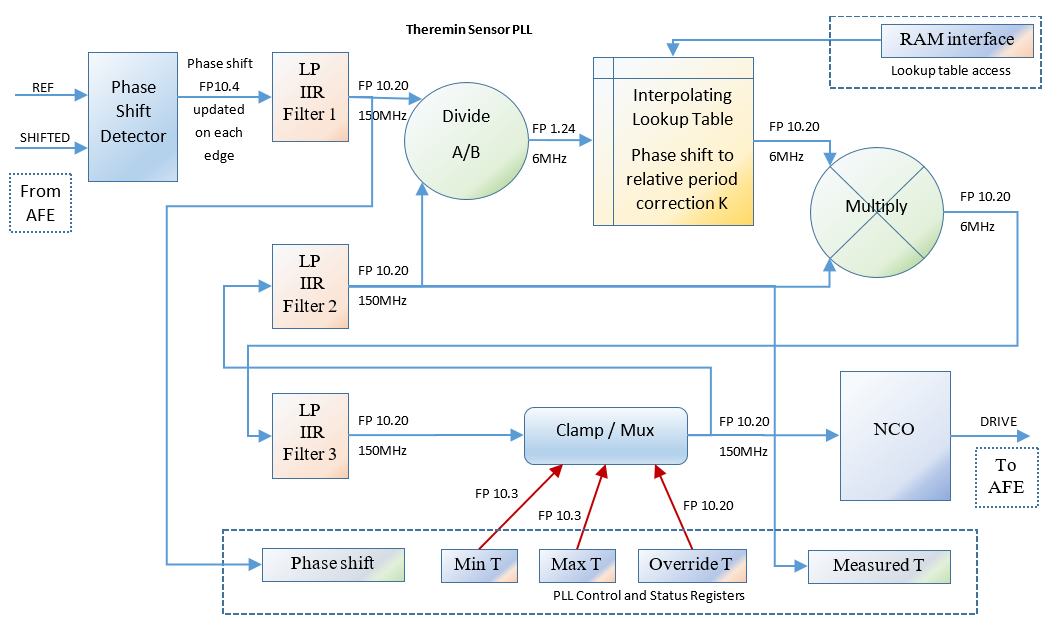
I'm going to profile F_drive/F_resonance to phase_shift during calibration and set interpolation table
based module which should calculate LC resonance frequency based on F_drive and phase_shift.


For the LCDPLL to be a low pass filter for phase noise, the integrated phase error should be used as the NCO input. 
The phase error is attenuated to set the loop bandwidth, and I use powers of 2 here because the bandwidth doesn't need to be any closer than that,
and right shifting to attenuate is free in digital logic.
-- dewster

I'm using the same approach for LP filters - right shift as filter K. What number of stages is reasonable?
I'm simulating filter response using Excel - as you suggested. For me, 2-stage response looks good.

I apply the 48kHz triangular dither directly to the NCO drive (frequency) control. 
-- dewster

Looks like the best point for adding dithering for me.


Then I'm looking at the phase difference between the two ends of the coil for 90 degrees, which is easily detected via XOR. 
I sample the phase inputs (via DDR) before XOR rather than after because the DDR elements are at the pins. 
I've got the dither frequency set significantly above the LCDPLL loop bandwidth so it isn't tracked by the loop. 
Too much dither (amplitude) can make the LC really bobble around, and I don't know how to quantify the upper limit of useful
dither (this is variable via a front panel knob, with 2x for each detent via shifting in digital logic).
-- dewster

I believe reasonable amount of dither should not go too far from resonance.

Did you see any difference in playing performance experience with high and low dither?


You can use an XOR if you generate an internal quadrature NCO signal,
I had code to do that at one point when I was still going down the heterodyning path IIRC. 
XOR is superior in this application because it is immune to edge noise (the NCO will be clean but the coil sense won't be) though
XOR can lock to harmonics.


One possible down side to single point sensing is: any differential
delay for the phase comparison paths can become a drift issue if it has any thermal dependency.
-- dewster

In my approach, generating of PI/2 phase inside NCO will cause phase drift.
In this case, serdes delay + FPGA output + comparator delay will be included into phase shift, and can vary, e.g. with current sensing comparator delay changes due to temperature drift.

To minimize phase drift, I'm using two identical comparators: one just sends drive signal back as is, and second - measures current.
I hope that drift in both paths will be the same, and will not affect phase difference seen by FPGA.

Since, I found method for phase shift measure near zero in FPGA, XOR will not give any benefits.

Posted: 6/4/2021 2:28:27 PM
dewster

From: Northern NJ, USA

Joined: 2/17/2012

"Then I can be sure that 1.2GHz resolution should be enough."  - Buggins

Totally enough.  At that resolution I think there will probably be enough environmental "dither" from the mains AC and such that you won't need to inject much, if any, to get rid of sticky points in the fields.

"Are you using Cyclone?  In Xilinx devices, even Spartan 6 has SERDES blocks."

Yes, Altera is unfortunately behind the times here.

"I'm using the same approach for LP filters - right shift as filter K. What number of stages is reasonable?  I'm simulating filter response using Excel - as you suggested. For me, 2-stage response looks good."

I'm using 5 stages in the FPGA hardware.  The first stage goes from 180MHz to 90MHz (Fc=244kHz) which makes the following 4 identical stages (Fc=207Hz) realizable in terms of timing.  It's probably overkill, but this puts any aliasing at 24kHz (Nyquist for the processor sampling) way down in the mud.  Each pole gives -20dB per decade, 207Hz to 24kHz is ~2 decades, and there are 4 poles, so -20dB * 2 * 4 = 160dB, which is over 32 bits of headroom at the processor register interface.  Overkill I suppose, but why not if the hardware is otherwise just sitting there?  Three stages would give 120dB, which is 32 bits.  You also might want to analyze the truncation noise in your filters (because you can't use the full width of the feedback).

"Did you see any difference in playing performance experience with high and low dither?"

I'm really not seeing the need for a lot of dither at all, at least in my "lab" environment.  Though when ContraDude was over for a demo the pitch field was acting a little weird.  I think that was due to flaky grounding and a noisy USB AC adapter, and a little dither seemed to get rid of it.

"Since, I found method for phase shift measure near zero in FPGA, XOR will not give any benefits."

XOR is nice because it compares two areas rather than two edges, so any edge noise won't cause mayhem, though duty cycle changes can.  If you're comparing two external in-phase signals then I'm not sure how you might use XOR as the sign of the phase error would be ambiguous.

Posted: 6/4/2021 2:52:14 PM
Buggins

From: Porto, Portugal

Joined: 3/16/2017


XOR is nice because it compares two areas rather than two edges, so any edge noise won't cause mayhem, though duty cycle changes can. 
If you're comparing two external in-phase signals then I'm not sure how you might use XOR as the sign of the phase error would be ambiguous.
-- dewster

In-phase comparision is about areas, too.
Phase sign is ambigous only if you don't know previous state. When two signals are different, sign depends on what was last two equal values - two 1s or two 0s.

Edge noise and duty cycle is compensated by averaging between two last edges.

Posted: 6/9/2021 2:23:38 PM
Buggins

From: Porto, Portugal

Joined: 3/16/2017

Proposed theremin sensor FPGA PLL diagram:


Analog frontend, as described in previous posts has one input and two outputs.

DRIVE - differential signal from FPGA to AFE : to drive LC tank
SHIFTED - differential signal from AFE to FPGA : current sensing based shifted signal
REF - differential signal from AFE to FPGA : feedback of DRIVE with delay introduced by the same components as drive buffer and current sensor

Time intervals below are being processed as fixed point values, integer part corresponds to number of 150MHz clock cycles.

NCO (numerically controlled oscillator) is implemented using OSERDES in DDR mode providing DRIVE output sampled at 1.2GHz rate.
Internal phase is stored as 10.20 fixed point value, and output is dithered to provide frequency close to requested.
NCO input contains clamping (to avoid generating signal with period outside min..max bounds) and override mux (allowing to override signal period with some value during calibration).

Inputs REF and SHIFTED are sampled using ISERDES shift register in DDR mode at 1.2GHz rate, then processed by phase shift detector.
Phase difference for single edge is 10.3 signed fixed point absolute shift value. Averaging for two recent edges gives 10.4 value which is updated once per edge.

IIR lowpass Filter 1 takes rarely updating (twice per signal period - e.g. 2MHz for 1MHz signal) fixed point 10.4 value and filters it providing additional bits from averaging.
Now we have longer filtered 10.30 signed absolute phase shift value.

Output of absolute phase shift LP filter is available in interface output register - for calibrating.

NCO drive period value is passed through LP filter 2 to simulate natural averaging inside LC and get effective averaged LC frequency value similar to LC behavior.

Divider takes phase shift and averaged NCO period value and calculates relative phase shift value: phase_shift / drive_period.
Divider output is 1.24 fixed point signed value - which gives -PI..PI phase shift value.
Since divider is implemented as shift + subtract, it takes N CLK cycles to produce N result bits.
For 25 division result bits, new value will be available only once per 25 CLK cycles (at 6MHz rate).

Lookup table with interpolator converts relative phase shift to drive signal period correction coefficient.
Table is being populated on calibration stage and represents LC tank Q related characteristics.
Lookup table BRAM requires interface with PS, to allow changing of table content.
Since input is updated once per 6MHz cycle, this module should perform processing at the same rate.
Linear interpolation is used to calculate smooth output value based on two sequencial table entries.
Output of lookup table is K such that drive_period * K is expected current LC resonance frequency period (K = LC_resonance_period / current_drive_period).

6MHz multiplier output is passed to LP filter 3, to smooth 6MHz transitions, and then used as NCO target drive period.

Either Filter 2 or Filter 3 output can be used as sensor output value (LC tank resonance frequency period as 10.20 fixed point with 150MHz CLK cycles as integer part).

During calibration, with hands far away from antenna, PS will override drive signal period to different values, and read measured phase shift.
Based on collected frequency / phase shift measurements, PS should populate lookup table with correction coefficients (actually shaped as atan() and scaled based on LC tank Q).

Once calibration is done and table if filled, overriding of NCO input is turned off, and PLL starts tracking LC resonance frequency (locking on it).
Since drive frequency is being updated slowly, high frequency noise will be filtered out.

Additional processing steps required for this sensor ouput:
Main hum noise filter (performed at LC drive period domain).
Linearization : conversion of period value (oscillator frequency) to hand-to-antenna distance - according to playable range settings.
Conversion of hand distance to note (for pitch antenna) or to volume (for volume antenna) - according to volume control settings.
These stages can be done at lower rate (e.g. at 48KHz audio sample frequency).

PCBs will be delivered soon, so I hope to start testing on real hardware in a couple of days.
So far, NCO, phase shift detector and divider modules are implemented and tested in simulation test bench.

Posted: 6/9/2021 3:35:47 PM
dewster

From: Northern NJ, USA

Joined: 2/17/2012

Wow Vadim, nice diagram!  And super complex DPLL!

When I was working on a sensor project, a Biology professor who was also working on it showed us some spreadsheet graphs he made, the results of which have really stayed with me.  We were debating how to measure and manipulate error, and his sample data showed that it didn't really matter much whether we took the difference of the direct data, or the difference of the inverse, exponential, etc. as long as it was over a fairly small interval.  I would submit that a Theremin DPLL is almost always locked, so the error is always small, so it doesn't need to be linearized or otherwise manipulated before being used as feedback.  Though I suppose the higher the Q and the lower the loop BW, the more one might want to do some linearization, as being off by even a little when the Q is high can dramatically lower the feedback gain, and hence the loop BW.

Another thing I learned from general PLL sims, way before I was thinking of Theremins seriously, was that bandwidth reductions in the loop can cause unintended instability or peakiness in the phase response, which is counter-intuitive.  I evidently worked in the same building with engineers who didn't understand this, as they had the VCXO supplier make special units with low pass filtering on the voltage control input (the way to control the bandwidth is via feedback, not LPF in the loop).

Posted: 6/9/2021 5:55:10 PM
Buggins

From: Porto, Portugal

Joined: 3/16/2017

I'm neither an electronics engineer, nor DSP expert. I'm trying to design sensor based on my poor knowledge.
Most likely, PLL design I'm proposing is not a PLL at all.

1) Let's consider case when drive signal has fixed frequency, and we are going to measure LC resonance frequency using only phase shift value.
If we know how phase shift changes with difference of drive frequency from resonance point, we can implement module which will calculate LC resonance frequency just from fixed drive frequency and phase shift.
I believe this approach can be usable (playable) if drive frequency is close to LC resonance for far hand distance (tune zoom region to far hand distance where we need max sensitivity).
Now we have a sensor which is working, and which is obviously not a PLL.

2) Then let's imagine that we've added a method to vary drive frequency slowly, trying to keep it closer to current LC resonance frequency (e.g by taking our calculated LC frequency, passing it via LP filter with low cutoff frequency. Since we change our drive frequency slowly, we still have mostly approach (1) with a kind of auto tuning or auto calibration.

3) Try to increase cutoff frequency for autocalibration LP filter to track LC resonance closer and faster.
I believe at some point this sensor would behave very close to PLL. But it's not a PLL. It's still phase shift basing sensor.

I think it's ok to have drive lowpass filter high enough to track speed of hand movement.


Posted: 6/9/2021 6:32:53 PM
dewster

From: Northern NJ, USA

Joined: 2/17/2012

There will be some variation in the phase detector gain due to the fixed system clock being used to measure period, but Theremin oscillators don't have to work over a very wide range so this can be ignored or designed around as worst-case.  Using a DPLL approach with high Q coils providing the voltage boost, you generally can't have people touching the raw metal antennas because the sense signal will hit the dirt, and then the DPLL will go out of lock and start hunting.  Touching the antenna is way beyond worst-case frequency drop for normal use, and a little insulation here is good for ESD too.

Then you have the pretty radical on-resonance gain of Q/pi, which absolutely must be figured into the design.  Off-resonance will substantially lower the loop gain and so lower the loop BW, but this only happens when the DPLL is out of lock (at start-up, or if someone touches a bare metal antenna).

Feedback in a DPLL is much like feedback in a digital filter, or in an op-amp.  It is negative to induce correction, and the overall loop gain must be less than 1 for stability.  The closer the gain is to one, the wider the BW and the less the inherent stability.  So the job really is just to calculate the individual gains of the phase detector, the NCO, the LC, and anything else in the loop, multiply them together, and do a simple z transform on the result (much like a first order digital LPF, you can do this easily in a spreadsheet and graph it).  Feedback loops give you the inverse of whatever is in them, so a LPF in the feedback loop will give you a HPF response, and vice-versa, you can see this directly in active analog boost / cut tone control circuits.

Posted: 6/9/2021 7:10:24 PM
Buggins

From: Porto, Portugal

Joined: 3/16/2017


Using a DPLL approach with high Q coils providing the voltage boost, you generally can't have people touching the raw metal antennas because the sense signal will hit the dirt, and then the DPLL will go out of lock and start hunting.  Touching the antenna is way beyond worst-case frequency drop for normal use, and a little insulation here is good for ESD too.
-- dewster


Couldn't limiting of drive frequency range (setting min and max period value for NCO after calibration) prevent from bad conditions when touching bare metal antenna?
I'm expecting that it will lock on min frequency (max period value) on touch.
Supporting of antenna touch is one of my goals.

BTW, can current sensing approach (one point connection to antenna via inductor) protect from ESD? Will ESD pass through inductor and keep high voltage on AFE side?
Anyway, I have ESD protection diode on analog frontend board...

Posted: 6/9/2021 7:26:18 PM
dewster

From: Northern NJ, USA

Joined: 2/17/2012

"Couldn't limiting of drive frequency range (setting min and max period value for NCO after calibration) prevent from bad conditions when touching bare metal antenna?"  - Buggins

It can help limit the out-of-lock hunting time.  I use an FPGA build parameter for this, it sets powers of 2 ranges for the minimum (max is whatever the NCO will do with max input).

"BTW, can current sensing approach (one point connection to antenna via inductor) protect from ESD? Will ESD pass through inductor and keep high voltage on AFE side?  Anyway, I have ESD protection diode on analog frontend board..."

I think it's probably safer than the C divider approach, but with ESD you can never be too careful.

Posted: 6/11/2021 4:33:31 PM
Buggins

From: Porto, Portugal

Joined: 3/16/2017

Received ordered PCBs from JLCPCB. Quality seems pretty good.

Manufacturing and delivery to Russia via HongKong post took ~20 days.

There are three boards: main board, LCD and controls board, and x2 sensor boards


Back side:

LCD and controls board design sizes are correct. Screen is centered.


LCD mounting holes at right places.

Encoders and pots placed at small interval. Need to find some solution for knobs. Ordered silicone vacuum caps - inner hole (6mm) is too wide (loose), probably due to shaft shape.

Going to search for 3D models and order 3D printing of knobs.

Main board with Z7-lite dev board on top.


A lot of soldering is waiting me...

You must be logged in to post a reply. Please log in or register for a new account.