Let's design and build cool (but expensive) FPGA based theremin

Posted: 1/18/2023 7:31:53 PM
Buggins

From: Porto, Portugal

Joined: 3/16/2017

OrangeCrab has a lot of resources (25K or 85K logic cells) but prices are a bit high (USD 95 / USD 150).
Main stopper probably is a low number of pins. How to bypass this limitation?
The board has USB connector. Controls and LCD which require a lot of pins may be replaced with Android phone or tablet running app with theremin UI, connected to FPGA board using USB OTG (via usb serial).
If no pins needed for encoders and LCD, feather form factor I/O is enough - for sensor analog front ends and audio I/O.
20 I/O pins available on OrangeCrab.
Let's try to distribute pins.
For advanced theremin sensor analog front end I'm going to design: (3+4)*2=14 pins for AFE with LVDS output (3 SPI with shared CLK for AD9833 sin wave drive generation, 4 for two LVDS pairs from reference and sensing comparator outputs).
Clock pin for DDS sine wave drive generator (25MHz) may be shared between two sensors, keeping 1 more pin.
6 pins left for audio I/O: 5 I2S (MCLK, LRCK, BCLK, DIN, DOUT), 1 S/PDIF out. With shared sensor clock pin, we can e.g. add S/PDIF input.
No pins left, e.g. we cannot use 2 pins for I2C control of audio codec (e.g. phones volume). Probably, 20 I/O is not enough.
Of course, using classic D-Lev AFE with 3 single-ended signals (drive, ref, sense), 8 more pins will still be available.


Another small but powerful Lattice based board (40K logic cells):

CRUVI Certus-NX Base Board with Lattice Certus-NX FPGA, 8 MB RAM, 4.5 x 5.7 cm
Certus NX LFD2NX-40-7BG196I FPGA


Found more interesting lattice boards:

Muse Lab iCESugar-Pro - 24K LUTs open source hardware, SO-DIMM form factor with a lot of I/Os for $55, or $71 with breakout board.


Muse Lab Colorlight
fpga LFE5U-45F-6BG381C 45k lut

25K LUT and 45K LUT boards (38 EUR, 54 EUR) available here


Posted: 1/20/2023 11:43:28 AM
Buggins

From: Porto, Portugal

Joined: 3/16/2017

So, there are 3 Lattice based FPGA boards from Muse Lab in SO-DIMM form factor, with compatible carrier boards.
All of them support open source toolchain, have big enough resources.
If you don't want to solder 0.4mm pitch SO-DIMM, ext board will work as a breakout.
I think it makes sense to consider it as D-Lev core board replacement in future version of D-Lev.
When 25K LUTs is not enough, 40K board may be used instead.

iCESugar Pro - LFE5U-25F-6BG256C 25K LUTS, 32MB SDRAM, 106 I/Os, 32MB SPI Flash, EUR 70 with ext board, EUR 55 w/o ext board:

Colorlight I5 - LFE5U-25F-6BG381C 25K LUTs, 8MB SDRAM, 2MB SPI Flash, EUR 53 with ext board, EUR 38 w/o ext board:

Colorlight I9 - LFE5U-45F-6BG381C 44K LUTs, 8MB SDRAM, 8MB SPI Flash, EUR 69 with ext board, EUR 53 w/o ext board:

Colorlight boards do not have on-board USB JTAG debugger, but have it soldered on ext board.
iCESugar Pro has JTAG debugger and Type C on SO-DIMM module, and one more on extension board. Docs say that additional JTAG may be used to debug softcore.
Colorlight boards instead of on-board debugger have two gigabit ethernet PHY chips, and one of 6 connectors is occupied by ethernet pins.
30-pin connectors are actually dual PMOD (6x2) on sides, with additional 4 I/O pins, GND and +5V.

Posted: 1/20/2023 6:24:55 PM
dewster

From: Northern NJ, USA

Joined: 2/17/2012

Looks like switching supplies?  Someone should test to see if that might be a problem or not.  Are there schematics for these anywhere?  I wonder what the I/O voltages are.

Posted: 1/23/2023 3:27:10 PM
Buggins

From: Porto, Portugal

Joined: 3/16/2017

iCESugar Pro schematic on github
All I/Os are 3.3V
Power supply uses switching regulators.

Colorful I5/I9 github repository is here
But it contains only schematic for extension board, not for FPGA board.
Both boards use switching regulators as well.
It's hard to find a board with linear regulators.


Just wondering, if it's possible to design your own FPGA base board and order assembly on JLCPCB, what would be the price?

Posted: 1/24/2023 3:20:40 PM
dewster

From: Northern NJ, USA

Joined: 2/17/2012

"Just wondering, if it's possible to design your own FPGA base board and order assembly on JLCPCB, what would be the price?" - Buggins

Last time I looked they had very little in the way of FPGA inventory to solder on there, and the prices were sky-high (mainstream FPGA pricing from legit suppliers is always insane).

Posted: 1/24/2023 7:19:59 PM
Buggins

From: Porto, Portugal

Joined: 3/16/2017


Last time I looked they had very little in the way of FPGA inventory to solder on there, and the prices were sky-high (mainstream FPGA pricing from legit suppliers is always insane).

Checked JLCPCB components available for assembly. No FPGAs. Even no chinese gowin FPGAs.

Another option - soldering by yourself.
I think, DIY soldering of QFN FPGA and other not too small SMD components is not a rocket science. But soldering of BGA - is...

Big enough Lattice FPGAs in qfn72 packages are in stock on Mouser at reasonable price. Gowin FPGAs in QFN88 packages - too.
Some QFP package devices are available as well - they have more I/O, but as well they are more expensive.

LCMXO3D-9400HC-6SG72C  $29  9K LUTs, QFN72, 58 I/O

LFXP2-17E-5QN208C $63 17K LUTs, PQFP-208, 146 I/O
GW1NR-LV9QN88PC6/I5  $34 8.6K LUTs, QFN88, 70 I/O
GW1NR-LV9LQ144PC6/I5  $38 8.6K LUTs, LQFP144, 120 I/O

GW1NR have embedded 8MB SDRAM, although SDRAM controller would eat ~800LUTs...

Easy to solder and cheap alternative to SDRAM is PSRAM with QSPI interface. It's probably enough for reverb and some other usage.

P.S.: It looks like it's possible to order 3d-printing of theremin cabinet on JLCPCB. It would cost about $100 in my estimation...

Posted: 1/25/2023 12:24:51 AM
Buggins

From: Porto, Portugal

Joined: 3/16/2017

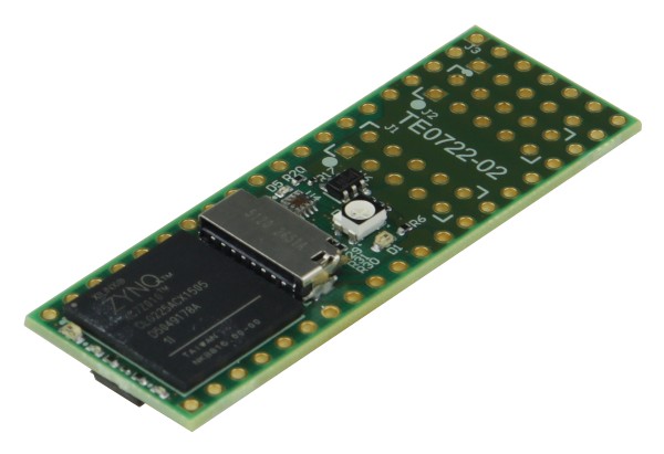
Trying to figure out if CMod A7-35T is suitable for digital theremin.

CMod A7-35T is small 48-pin DIP board based on Artix 7 FPGA with 20K LUT6, 40K FFs, 225KB block RAM, 90 DSP slices.

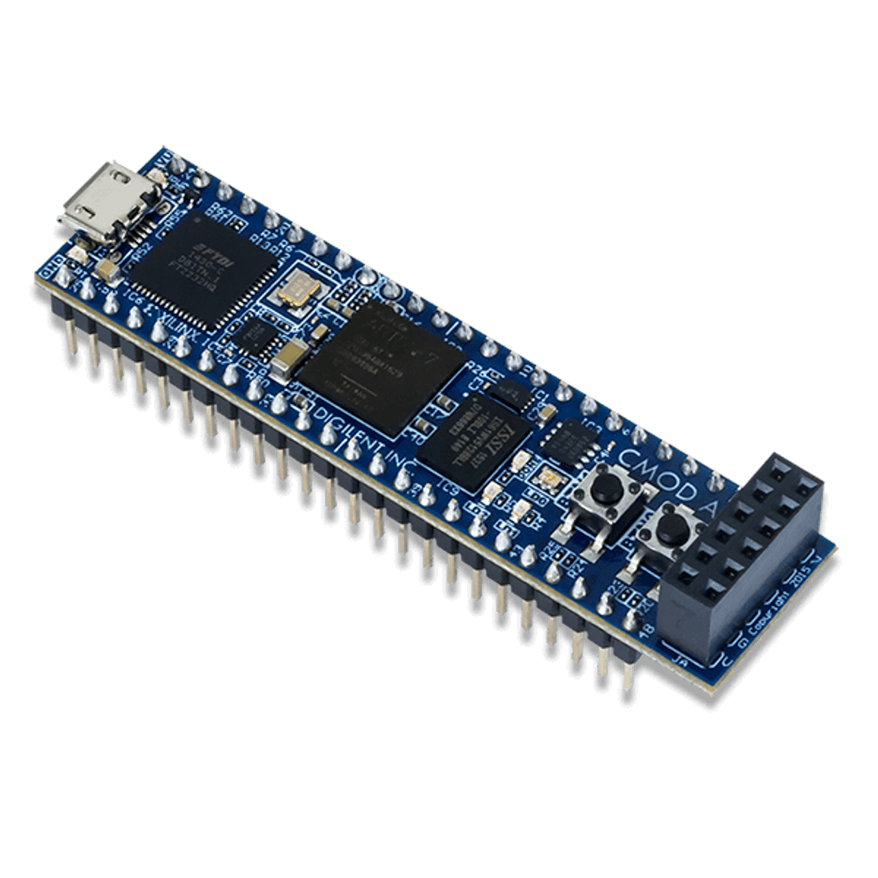
Provides 44 digital I/O pins, and 2 ADC inputs via 48pin headers, and 8 I/O pins via PMOD connector.
In stock on mouser and digikey for $100.


Has on-board 512KB SRAM chip with 8-bit interface and 125MHz max clock.
On board 4MB QSPI flash - for configuration. Part of it can be used as user storage (bitstream takes about 18Mbits, leaving ~14MBits free).
Probably, it would be possible to update configuration bitstream in QSPI flash from PC using FPGA (softcore CPU) - in this case no JTAG programming tools will be needed for updating of bitstream.
MicroUSB connector for power, JTAG, and serial. Can be programmed via USB. Configuration / presets may be uploaded to board using usb-serial.

Of course, unfortunately, this board has switching power supply (LTC3569).


Let's try to figure out if CMod A7 has enough pins to implement theremin of dream.

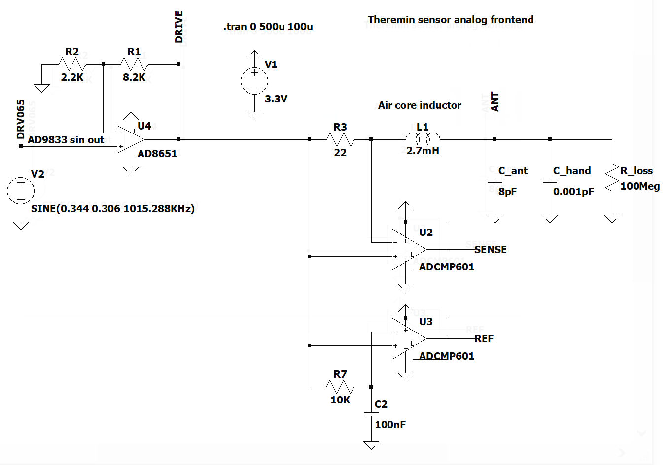
The heart of theremin is a sensor. Two sensors.
Cool sensitive and noise immune sensor I'm planning to use will be a PLL front end with current sensing, direct digital synthesis based pure sine wave drive signal (AD9833), opamp buffer/amplifier for drive signal, two comparators with LVDS outputs - one for reading of drive signal (REF), and second for current sensing (SENSE).
REF and SENSE lvds outputs will occupy 4 pins of FPGA per sensor. LVDS input on 3.3V bank of Xilinx Series 7 FPGA is working only with external terminating resistor.
AD9833 needs one 25MHz clock for ACD/DDS, and 3 signals for SPI control interface (CLK, CS, MOSI) to update DDS frequency.
Let's provide differential clock signal to sensor AFE to minimize noise.
The same clock may be reused for both DDS and SPI control interface. Xilinx Series 7 3.3V I/O bank cannot provide LVDS output, but we can just output complementary signal on two CMOS33 pins and then receive it in sensor using comparator.
So, 2 pins shared between both sensors will be used as differential clock.
As well, we will need 2 output pins for SPI - CS and MOSI (SPI CLK is shared with DDS clock).
Total number pins required for two sensor AFEs is (2+2+2)*2+2 = 14
Probably this approach is an overkill, and too expensive, but I really want to try it.

Audio interfaces are also important.
For high quality I/O we can put S/PDIF input and output modules - 2 pins.
As well it's useful to have analog audio connectors - Line Out, Line In, Mic In, Phones.
For analog part let's use SGTL-5000 audio codec IC.
It will need 5 pins for I2S interface (MCLK, LRCK, BCLK, DIN, DOUT) and either 2 pins for I2S (SCK, SDA) or 3 pins SPI (CLK, CS, MOSI) - mostly to control phones volume.
Connecting SGTL5000 using SPI control would take 5+3=8 pins.

Cool theremin needs touch screen.
4.3 inch 800x480 capacitive touch LCD module from Waveshare looks like a good choice.


4 pins will be used as LCD clock and sync (HS,VS,DE,PCK).
16M colors RGB888 needs 24 pins just for color information. Less colors would be ok for us.
12bit 4K colors (RGB444) should be enough.
Capacitive touch uses SPI interface (CLK, CS, MOSI, MISO) and two additional signals (RESET, IRQ).
Not sure if RESET is really required. Probably, it can be just pulled up or down.
Probably, we can leave w/o IRQ pin (polling via SPI may be enough?).
So far, let's count pins including IRQ and RESET.
4K colors touch LCD will occupy 12+4+4+2 = 22 pins.

But some SPI pins (CLK, MOSI) may be shared between audio (SGTL5000) and touch controller.
In this case, RGB touch LCD will consume 20 pins.

So far, sensors + audio + LCD occupied 14+8+20 = 42 of 44 digital I/O pins available on DIP headers.
How can we spend 2 more digital pins?

We don't have hardware controls like buttons and encoders so far.
2 pins seems like a bottleneck. But we still can add a lot of rotary encoders and buttons.
Let's use serial connection with encoders and buttons board.
Shift registers with parallel inputs and serial output may help us.
8-bit shift register gives ability to read 8 inputs. Several registers may be connected in chain to increase number of inputs.
One encoder with pushbutton has 3 outputs to read. 6 such encoders need 6*3=18 inputs - three 8-bit shift registers will be used (the rest 6 or 7 inputs give the ability to add 6 or 7 buttons or 2 additional encoders).
LOAD signal will latch input state into all registers.
SHIFT signal will shift out latched pins state bit-by-bit
OUT signal will be used to read serial data
Of course, for reading of 24 inputs via 3 wires we will need 24 SHIFT signal pulses and one LOAD cycle.
So, 3 pins for reading of huge amount of buttons and encoders is enough.
But we have only 2 pins left unused on DIP header.
Let's just reuse some existing signal as CLK for encoders interface. E.g. it may be CLK from SPI or some clock from audio I2S interface (e.g. 48KHz LRCK gives 48000/24=2000 times per second scan rate of encoders synchronous to audio sample rate simplifies filtering out of noise from this shift register chain).

There are still two unused pins on DIP header - dual ADC pins.
We can use analog ADC pin for pit (e.g. phones volume control).
We can use analog ADC pin to read state of expression pedal (with pot inside).
Two reasonable options:
- Two pots (e.g. phones volume + reverb/effect)
- Phones volume pot + pedal
- Two pedals

It looks like DIP header of CMod A7 board provides enough pins for our cool theremin.

What about resources?

For LCD it's nice to have enough memory for framebuffer.
Onboard 512K SRAM can fit 800x480x8bit framebuffer.
To provide 12bit RGB444 from 8bit pixel we can use palette.
Or we can limit number of colors even more, to 8bit RGB (3-3-2) - it would free 4 more pins.
If we didn't need framebuffer, 512K might be used as data or code RAM for soft core - to fit bigger program.
Or, we could use it as a buffer for reverb (~5 seconds).

Unfortunately, we don't have enough free pins to connect external big RAM - for framebuffer and reverb buffer.
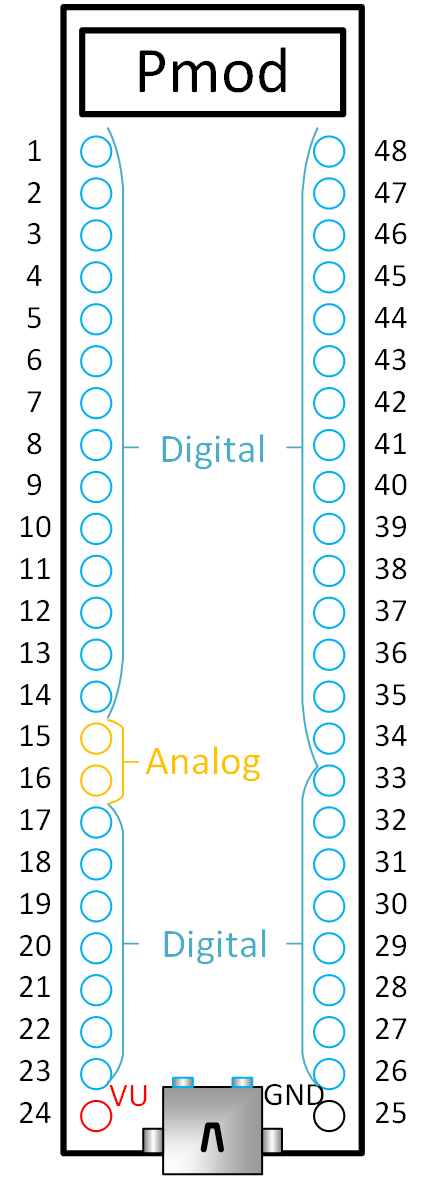
But there is a PMOD connecter, soldered with a bit strange orientation. It has 8 digital I/O pins inside.
Can we connect RAM to it?
We can connect PSRAM chip with QSPI interface using 6 pins of PMOD header.
Cheap 8MB PSRAM in 8-pin package are available.
Even with 100 or 133MHz clock and using QSPI mode (4-bit transfer per clock cycle and 50 megabytes per second throughput) it will be slow enough due to big latency (read and write operations take a lot of cycles).
But if batch read or write is ok (like for fetching pixel data for LCD), QSPI PSRAM seems to be useful.

Two more free pins on PMOD header.
We can use them as additional CS for SPI interface - to connect more SPI or QSPI devices.
E.g. additional QSPI Flash, and/or SD card.

Conclusion.
CMod A7-35T is good enough for usage as Digital Theremin core.
Pros:
      a lot of FPGA resources (20K LUT6 is much more than 20K LUT4 of competitors, it's closer to 40K LUT5 + 40K FFs, 90 DSPs - just unbeatable)
      always in-stock!!!
      easy to solder connectors
      now $100 price does not look too big anymore (Artix 35 chip costs about $80)
      I'm familiar with Xilinx tools
Contras:
      switching power supply
      small size of onboard SRAM


Posted: 1/26/2023 7:18:08 PM
dewster

From: Northern NJ, USA

Joined: 2/17/2012

Interesting find and analysis Vadim!  I guess the touch display eating so many pins is OK if it is the main I/O.  The thing I don't like about these LCDs is they really wash out in bright light, whereas the old school LCDs work in both transmissive and reflective modes.  You could put an image of the tuner or equivalent on the screen though, which would be nice.  It's great for us that general interest in soft RISC-V is spawning a bunch of FPGA hobby boards.  Just wish they were a bit bigger to utilize more of the stranded FPGA I/O, the degree of miniaturization they all seem to strive for is a little on the nuts side.

Posted: 1/30/2023 6:04:23 PM
Buggins

From: Porto, Portugal

Joined: 3/16/2017


Interesting find and analysis Vadim!  I guess the touch display eating so many pins is OK if it is the main I/O. 
The thing I don't like about these LCDs is they really wash out in bright light, whereas the old school LCDs work in both transmissive and reflective modes. 
You could put an image of the tuner or equivalent on the screen though, which would be nice. 
It's great for us that general interest in soft RISC-V is spawning a bunch of FPGA hobby boards. 
Just wish they were a bit bigger to utilize more of the stranded FPGA I/O, the degree of miniaturization they all seem to strive for is a little on the nuts side.

Are you going to use theremin on the sun?

There are some e-ink screens available, reflective and with good viewing angle. But they are slow - not suitable for tuner (0.3s .. 3s lag).
Actually, speed of Theremini LCD is closer to e-ink than to LCD


Yet another strange solution for fpga theremin core board, available in stock for ~$120.

DIPFORTy1 "Soft Propeller" $120 Xilinx Zynq-7: XC7Z010-1, 16MB SPI Flash, 33.3333MHz clock, Dual Core ARM


FPGA part of Zynq7010 SOC has the same resources as Artix-35.
No external memory, but for some cases 256KB of on-chip memory can be enough.
34+6+4=44 I/O pins available (3.3V).
Has SD card slot.
3.3V external power supply. Two switching regulators for internal 1.8 and 1.0 voltages.
No on-board USB serial for connection to smartphone or tabler as GUI/control.
No on-board USB JTAG for programming. Programming requires external JTAG.

Posted: 3/1/2023 5:12:42 PM
Buggins

From: Porto, Portugal

Joined: 3/16/2017

Experiments with simulation of AD9833-based DDS sine wave drive analog front end in fixed drive frequency mode with phase shift measurement.

LTSpice model (github download link):


AD9833 sine wave output has 0.612V peak-to-peak swing with 0.344V middle point.
It should be amplified and buffered by opamp (to 0.3..3.0V swing).

Inductor has 120 Ohm series resistance. Antenna self capacitance is 8pF. Antenna voltage swing is 300Vpp for such a high inductor resistance.
Assuming that hand hear antenna gives 2pF of additional capacitance, and each 10cm of distance reduces hand capacitance by 4 times.
Current sensing uses R_sense (R3) is 22 Ohm.

One comparator is used for sensing - compares voltage on two sides of R_sense - provides SENSE output signal.
Second comparator is used to get generated drive signal as square wave REF. It compares drive signal with its LP-filtered copy. Is there some better solution for providing reference voltage for REF comparator?
Sine drive signal is tuned to value close to LC resonance - 1015.288KHz

Excel table with results (github download link):


Chart 1. phase shift measured between REF and SENSE signals for different hand distances:

Chart 2. antenna voltage swing for different hand distances:

Chart 3. capacitance added by hand (pF) for different hand distances:

The lower voltage swing on R_sense is, the slower is change of SENSE comparator output.
Probably, it's the reason of phase shift > 90 degrees.

Drive signal frequency may be set to value higher than phase-0 point, still fitting into area with high antenna swing.

By 60cm hand distance, phase shift is reduced to 1ns per 10cm of distance.
Averaging has to provide 10-12 additional bits to make this distance playable.

As for me, fixed drive, phase shift measurement theremin sensor should work good enough.
I believe, there is no sensitivity difference for far hand distance between fixed drive and PLL drive approaches.

You must be logged in to post a reply. Please log in or register for a new account.