Teensy 4.0 600MHz ARM Cortex M-7 MCU - ideal for digital MCU based theremin?

Posted: 11/24/2019 9:09:50 AM
Buggins

From: Porto, Portugal

Joined: 3/16/2017

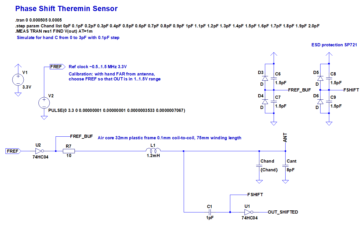
Collected data from RC delay between output and input.

It's not "dithered", but looks like alternating between two values with small frequency.

Pairs of raising pos, falling pos - captured for each cycle (~690KHz).

Code:
137 29
137 29
137 29
137 29
137 29
138 29
138 29
138 29
138 29
138 29
138 29
138 29
138 29
138 29
138 29
138 29
138 29
138 29
138 29
138 29
138 29
138 29
137 29
137 29
137 29
137 29
137 29
137 29
137 29
137 29
138 29
138 29
138 29
138 29
138 28
138 28
138 28
138 28
138 28
138 28
138 28
138 28
138 28
138 29
138 29
138 29
138 29
137 29
137 29
137 29
137 29
137 29
137 29
137 29
137 29
137 29
137 29
137 29
137 29
137 29
137 29
137 29
137 29
137 29
137 29
137 29
137 29
137 29
137 29
137 29
137 29
137 29
138 29
138 29
138 29
138 29
138 29
138 29
138 29
138 29
138 29
138 29
138 29
138 29
138 29
138 29
138 29
138 29
138 29
137 29
137 29
137 29
137 29
137 29
137 29
137 29
137 29
138 29
138 29
138 29
138 29
138 28
138 28
138 28
138 28
138 28
138 28
138 28
138 28
138 29
138 29
138 29
138 29
138 29
137 29
137 29
137 29
137 29
137 29
137 29
137 29
137 29
138 29
138 29
138 29
138 29
138 29
138 29
138 29
138 29
138 29
138 29
138 29
138 29
138 29
138 29
138 29
138 29
138 29
137 29
137 29
137 29
137 29
137 29
137 29
137 29
137 29
137 29
137 29
137 29
137 29
137 29
137 29
137 29
137 29
137 29
137 29
137 29
137 29
137 29
137 29
137 29
137 29
137 29
138 29
138 29
138 29
138 29
138 30
138 30
138 30
138 30
137 30
137 30
137 30
137 30
137 29
137 29
137 29
137 29
137 29
137 29
137 29
137 29
137 29
137 29
137 29
137 29
137 29
138 29
138 29
138 29
138 29
138 29
138 29
138 29
138 29
137 29
137 29
137 29
137 29
137 29
137 29
137 29
137 29
138 29
138 29
138 29
138 29
138 29
138 29
138 29
138 29
138 29
138 29

There is internal feature in Teensy 4 PWM - similar to dithering, can be applied to output signal raising and falling edge position as fractional part (5 bits).
It's not oversampling. It's a kind of dithering - 1 is added to position value for A of 32 cycles - if fraction is set to A/32.
Not sure if it's dithered or goes as single piece once per 32 cycles.

Posted: 11/24/2019 3:35:12 PM
dewster

From: Northern NJ, USA

Joined: 2/17/2012

The dither on the D-Lev started out as pseudo-random noise and ended up a 48kHz triangle wave.  I suppose the triangle wave could alias with environmental interferers, but the dither itself is largely zeroed out due to the DPLL sampling rate also being 48kHz.  Dither is more necessary for square waves, where all of the phase information (and thus any phase error) is concentrated in just two edge events per cycle.  If you could get the dither rate to match your sample rate you'd be golden.

Posted: 11/25/2019 12:46:34 PM
Buggins

From: Porto, Portugal

Joined: 3/16/2017


Dewster: If you could get the dither rate to match your sample rate you'd be golden.


I can use x32 dithering of reference signal phase and then use averaging window K*32 - this should filter out dithering noise completely.

I've tried output of logic to inductor and remove resistors before output signal buffer as you suggested, and found that it works well in LTSpice simulation.

Schematic has been simplified a lot (mainly due to square to sin convertion removed).


With max Q (no damping resistors or caps), it's still usable: good "zoom" of 0.1pF C_hand range corresponding to far hand distance (>21cm) - it's ~6% (1/16) of range.[/font][/size][/color]
Although there is a distortion before resonance (increasing of C not always increases phase shift), for C_hand > C_resonance everything is ok.

In this simulation, C_hand is being changed 0.0..2.0 with 0.1pF step.

Widest 0.1pF step near resonant frequency will be tuned for max hand distances.


Voltage swing on antenna ~200V looks scary for me. Won't it kill 1pF capacitor?

As usual, LTSpice model is available on GitHub

KiCad project is available on GitHub, too.

Schematic screenshot from KiCad:

3d render of PCB:

Posted: 11/25/2019 2:06:54 PM
dewster

From: Northern NJ, USA

Joined: 2/17/2012

"I can use x32 dithering of reference signal phase and then use averaging window K*32 - this should filter out dithering noise completely.  - Buggins

The slower the better if you want the output dither to make it through the LC network and dither the input.  I was using differentiated noise for dither and the LC filtered it all out.  Even the 48kHz triangle wave dither gets filtered out more than I would like.

"Voltage swing on antenna ~200V looks scary for me. Won't it kill 1pF capacitor?"

I'm using tiny little capacitors that came in an assortment from Radio Shack or China for the 1pF which can't be rated for more than 25V or so but they seem to be able to handle many times that.  I wouldn't put that in production, but it seems to work OK for experimental purposes.  For production you could use a series combination of 5 x 4.7pF or similar.  You could leave room and pads on your PWB for that.

So you're relying on the ESD protection to clamp and protect U1?  You might try a large value resistor across U1 I/O (220k or 470k) in an attempt to formally center up the non-clamped region of operation.  And I would probably also put a small value resistor in series with U1 input just to protect the protection diodes inside (guarantee that the ESD protector is doing all the work).

I haven't tried your simulation though.  Also, you can include component models in the schematic itself, I often do that when they are external to the LTSpice libraries just to make it easier on others.

Your PWB is rendering is really pretty!  Will you socket the ICs?  I would socket all the actives, as well as the 1pF, and perhaps the 10 ohm.  Are you using less "Q-killing" coil series resistance now?

Posted: 11/25/2019 3:54:57 PM
Buggins

From: Porto, Portugal

Joined: 3/16/2017

"I can use x32 dithering of reference signal phase and then use averaging window K*32 - this should filter out dithering noise completely.  - Buggins

The slower the better if you want the output dither to make it through the LC network and dither the input.  I was using differentiated noise for dither and the LC filtered it all out.  Even the 48kHz triangle wave dither gets filtered out more than I would like.


Unfortunately periodic x32 dithering is the only option available on Teensy 4 w/o additional hardware or software resources.
Alternative solution - use I2S LRCK (44100Hz) to form some signal to mix in.

"Voltage swing on antenna ~200V looks scary for me. Won't it kill 1pF capacitor?"I'm using tiny little capacitors that came in an assortment from Radio Shack or China for the 1pF which can't be rated for more than 25V or so but they seem to be able to handle many times that.  I wouldn't put that in production, but it seems to work OK for experimental purposes.  For production you could use a series combination of 5 x 4.7pF or similar.  You could leave room and pads on your PWB for that.

So far, changed 1pF to 2 * 2.2pF

So you're relying on the ESD protection to clamp and protect U1?  You might try a large value resistor across U1 I/O (220k or 470k) in an attempt to formally center up the non-clamped region of operation.  And I would probably also put a small value resistor in series with U1 input just to protect the protection diodes inside (guarantee that the ESD protector is doing all the work).

Updated schematic - 2 x 1Meg centering resistors + 100 Ohm protective resistor. Seems working fine.
I've removed centering resisters due to your objections regarding auto-centering by ESD diodes.
But actually, once voltage falls below 3.3+0.7V, centering would break w/o resistors.

I haven't tried your simulation though.  Also, you can include component models in the schematic itself, I often do that when they are external to the LTSpice libraries just to make it easier on others.Your PWB is rendering is really pretty!  Will you socket the ICs?  I would socket all the actives, as well as the 1pF, and perhaps the 10 ohm. 

So far, I'm not going to use sockets - since don't have them. BTW, what is the best socket to use for prototypes? Are there sockets for passive components as well?

I don't know how to include used component models (in this schematic, it's only 74hc74) into .asc
Is there any tutorial?


Are you using less "Q-killing" coil series resistance now?

I'm trying to achive the best Q possible.

Killing of Q reduces "zoom" - sensitivity for far distances / small C.
I'm calculating (max 0.1pF step) / (F_ref period).
Some results for different R_q:
1: 4.9%
10: 6.5%
22: 5.7%
47: 5.8%
100: 5.0%
Current through R (and IC out) is ~8mA for small R, and 6mA for R=100
Looks like max sensitivity is near 10-20 Ohm "killing Q" resistor.
Probably, small R won't protect IC output well enough.
Actually, difference between 5 and 6.5% is not too big.
"Killing Q" might be required to keep value for close hand distance (C_hand ~ 1.5pF) in "smooth" range. Smoothness may be broken during transition between "clamping" and "non-clamping" modes.

You've described "voltage dumping" effect in one of replies. Is it something additional to predicted dumping due to out-of-resonance and increased C (behavior modelled by LTSpice)?


Updated model (and 74hc74.asy with 74hc.lib) is available here

Direct link to raw phase_shift_sensor_v4_optimization_1200uH_resistors.asc

Updated PCB layout:

Posted: 11/25/2019 5:14:14 PM
dewster

From: Northern NJ, USA

Joined: 2/17/2012

"But actually, once voltage falls below 3.3+0.7V, centering would break w/o resistors."  - Buggins

Yes, good point.

"So far, I'm not going to use sockets - since don't have them. BTW, what is the best socket to use for prototypes? Are there sockets for passive components as well"

I "roll my own" IC and passive sockets out of single line socket stock.  That way you don't have to keep a ton of different sockets on hand, just snap off whatever you need:


"I don't know how to include used component models (in this schematic, it's only 74hc74) into .asc.  Is there any tutorial?"

You copy and paste the .MODEL text into the schematic, as "SPICE directive" text.  Not sure with .CIR or .SUBCKT, I don't think I've ever done that.

"Smoothness may be broken during transition between "clamping" and "non-clamping" modes."

This seems like it might be the scariest part of this approach.

"You've described "voltage dumping" effect in one of replies. Is it something additional to predicted dumping due to out-of-resonance and increased C (behavior modelled by LTSpice)?"

By "voltage dumping" do you mean diminished amplitude of antenna swing voltage?  There is, as you say, reduced swing due to off-resonance LC (determined by total Q of the LC and distance from the LC resonance frequency).  I believe increasing hand C may reduce the amplitude as well, particularly if the drive and coil resistances aren't super low.  A third factor is the electrical resistance of the human body, which the hand C is in series with, which damps LC resonance.  I can observe this directly on the D-Lev as resonance is perfectly (more or less) maintained.

Posted: 11/25/2019 5:36:46 PM
Buggins

From: Porto, Portugal

Joined: 3/16/2017

I "roll my own" IC and passive sockets out of single line socket stock.  That way you don't have to keep a ton of different sockets on hand, just snap off whatever you need

Thank you for pointing at this! Will buy them next time while visiting local electronic components store.


You copy and paste the .MODEL text into the schematic, as "SPICE directive" text.  Not sure with .CIR or .SUBCKT, I don't think I've ever done that.

74hc74 is .SUBCKT

Code:
* Inverter gate
* tpd 25n/9n/7n
* tr 19n/7n/6n
.SUBCKT 74HC04  A Y  VCC VGND  vcc1={vcc} speed1={speed} tripdt1={tripdt}
.param td1=1e-9*(9-3-3)*4.0/({vcc1}-0.5)*{speed1}
*
XIN  A Ai  VCC VGND  74HC_IN_1  vcc2={vcc1}  speed2={speed1}  tripdt2={tripdt1} 
*
A1  Ai 0 0 0 0  Yi 0 0  BUF  tripdt={tripdt1}  td={td1}  
*
XOUT  Yi Y  VCC VGND  74HC_OUT_1X  vcc2={vcc1} speed2={speed1}  tripdt2={tripdt1}
.ends


But it has symbol as well


Code:
Version 4
SymbolType CELL
LINE Normal -16 80 -16 48
LINE Normal 64 64 32 64
LINE Normal -16 80 16 64
LINE Normal -16 48 16 64
LINE Normal -16 64 -48 64
CIRCLE Normal 32 72 16 56
WINDOW 0 -16 32 Left 0
WINDOW 3 -32 96 Left 0
SYMATTR Value 74HC04
SYMATTR Description Inverter gate
SYMATTR SpiceLine VCC=5  SPEED=1.0  TRIPDT=1e-9
SYMATTR Prefix X
SYMATTR SpiceModel VCC 0
SYMATTR ModelFile 74HC.lib
PIN -48 64 NONE 8
PINATTR PinName A
PINATTR SpiceOrder 1
PIN 64 64 NONE 0
PINATTR PinName Y
PINATTR SpiceOrder 2


So far, here is download link for 74hc.lib and 74hc74.asy
If placed near .asc file, makes it work.


One thing I'm unsure is if I specified inductor parameters correctly or not. (I've started separate thread with question about LTSpice inductor params and Coil64).

In recent model, I'm using 1.2mH inductor on 32mm frame air core, 75mm winding of 0.2mm copper wire.
I specified 24.4 series resistance, 1.779Meg parallel resistance, 1.343pF self capacitance.
Not sure about parallel resistance. Probably it should be bigger for this coil.

Posted: 11/26/2019 6:46:25 AM
Buggins

From: Porto, Portugal

Joined: 3/16/2017

Dewster,

Isn't this this kind of socket better for DIP ICs?

Posted: 11/26/2019 12:31:16 PM
Buggins

From: Porto, Portugal

Joined: 3/16/2017

SP721 and 74HC04 input capacitance is working as voltage divider (3pF ESD + 3.5pF HC04) / 1pF
So, input is reduced by 6.5 times before clamping. Increasing of 1.0pF C on buffer input would reduce divider, but will harm overall sensitivity (reduce reaction of LC frequency on change of C_hand).

What about switching to more fresh hardware?
There are ESD protection devices with C 1pF or less, and tiny fast inverters with C 2.5pF
E.g., NC7WZ04 as 2-channel inverter (2.5pF), and IP4220CZ6 (1pF) as 4-channel ESD (it's what is available in local store).

I've updated Inductor parameters (1.2mH 0.2mm wire 75mm winding on 32mm frame) based on working frequency and Coil64 calculations.
Changed ESD capacitance from 3pF to 1pF, connected 2.5pF cap instead of inverter input.
Instead of 1pF on input, I'm using 0.73pF=2.2pF/3 - 3 sequential 2.2pF caps.
It gives 9.5% sensitivity (widest 0.1pF C_hand output range - relative to reference frequency period) - vs 5-6% before. I believe it's equivalent of +5cm of hand distance with the same sensitivity / latency, or just twice smaller quantization for the same distance.

+-170V (340V) on antenna. Nice transmitter.

Posted: 11/26/2019 4:00:59 PM
Buggins

From: Porto, Portugal

Joined: 3/16/2017

Experimented a bit more.
It's easy to achieve 8-9 % of range for 0.1pF C_hand interval near resonance.

But I found interesting thing after increasing VCC of invertor which drives L from 3.3 to 5V (leaving VCC of the rest at 3.3)
Got +-300V on antenna and really high Q (zooming of middle interval) - 14.5%
But buffer output current is 25mA with R_q = 0. With R_q=100, antenna voltage returns to +-150V which we had with 3.3V drive via R_q=0, but zoom is still good enough - 11.5% and drive current is back to 12mA


You must be logged in to post a reply. Please log in or register for a new account.