Armstrong, Hartley, Colpitts, Clapp, Wallin...

Posted: 11/17/2021 5:47:56 PM
Buggins

From: Porto, Portugal

Joined: 3/16/2017

Trying to simulate main hum noise in LTSpice.
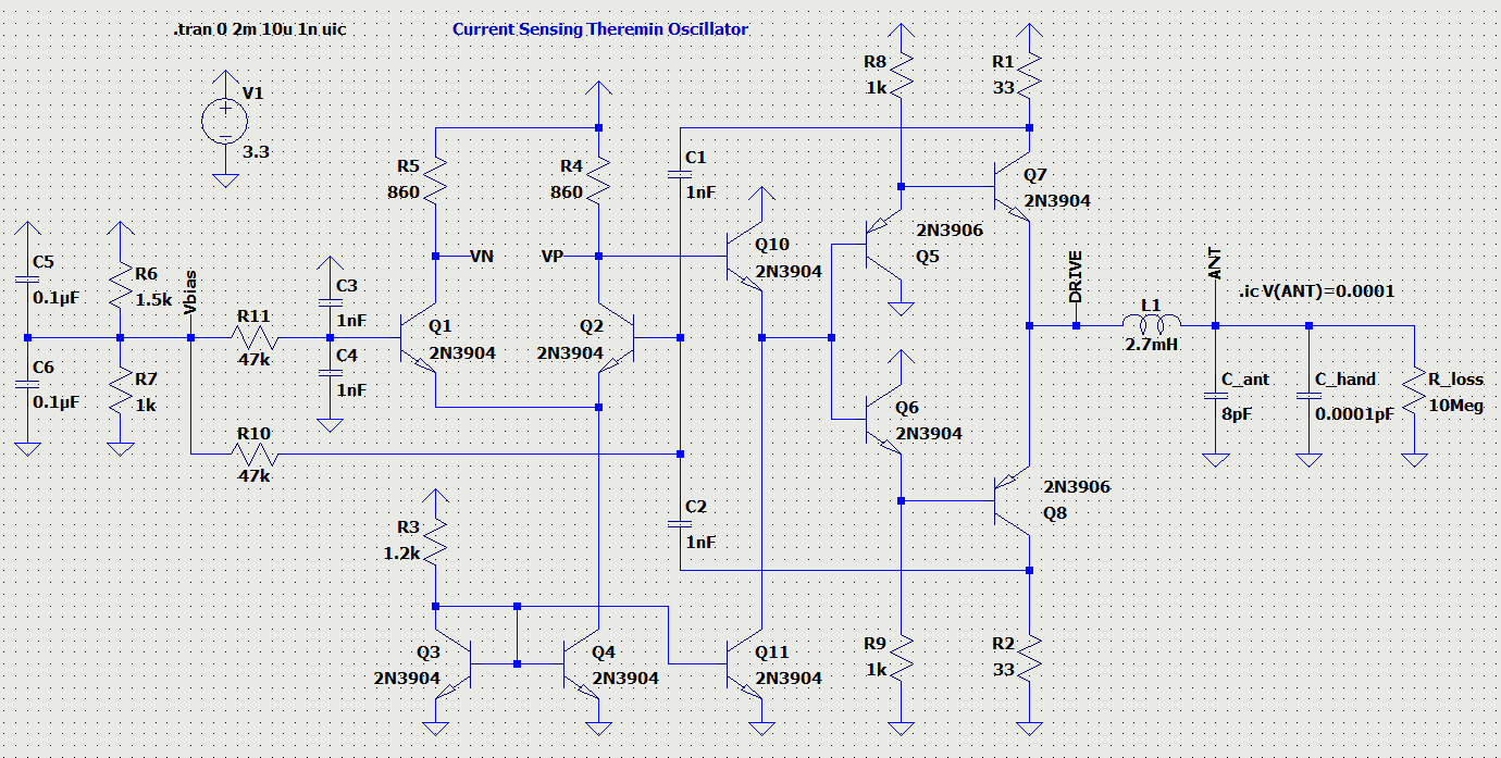
Using my recent model with 4 BJT both rail sides current sensing, and dual unbuffered LVC inverters as drive.
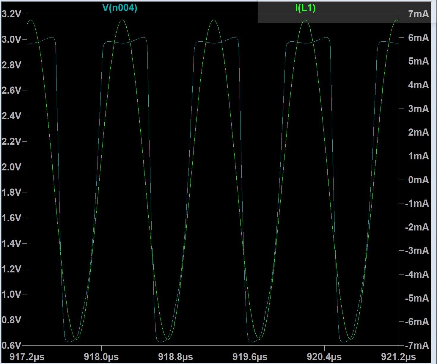
Connected C_ant to 100Hz 240Vpp voltage noise simulation instead of GND. 100Hz is used instead of 50/60Hz to speed up simulation. It should be better visible in oscillator anyway.
Noise period is 10ms. Let's try to simulate scope with trigger delay 1/2 of main hum period = 5ms.

Steps:

1) go to starting point 1ms
2) find nearest raising edge intersection with 1.65V: point 1.000667683
3) add half of noise period = 5ms
4) display current waveform for found point + 2us (in our case it's 6.000667683ms to 6.002667683ms, voltage axis set to 0.8..2.5V)
5) take screenshot of waveform, paste as new layer in GIMP
6) repeat steps 1..5 for other points, with 1ms steps
After adding new layer, align it above layer below based on plot frame
As a result, I've taken waveforms for 5 time intervals:

6.000667683ms 6.002667683ms
7.000366957ms 7.002366957ms
8.000066231ms 8.002066231ms
9.000858077ms 9.002858077ms
10.000557358ms 10.002557358ms


Resulting image for single trace (at 6.000667683ms)


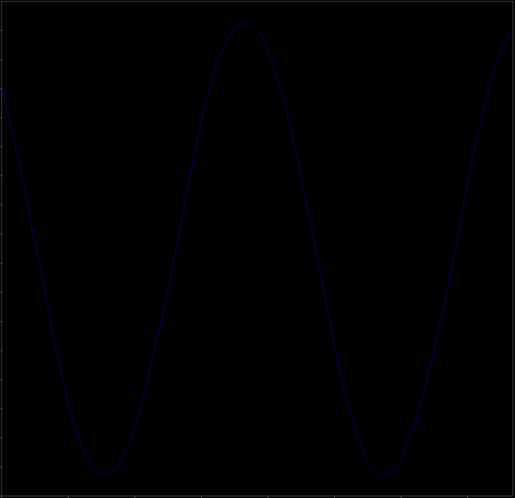
5 layers combined with "lighten" mode

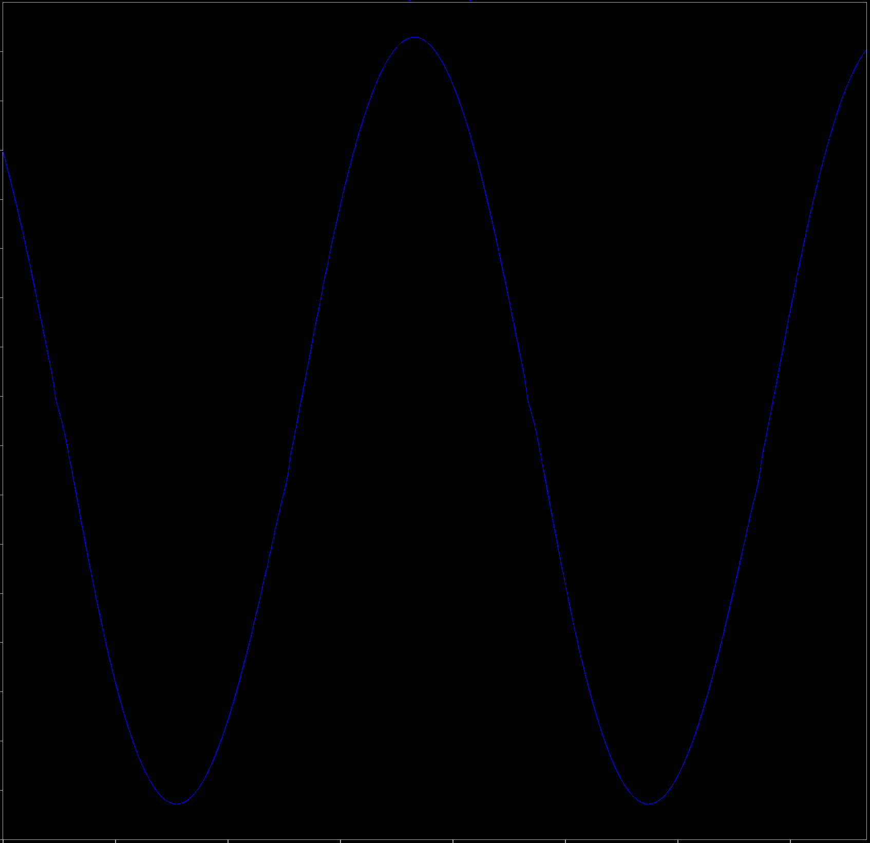
I don't see any visible noise. It looks like main hum is not a changing "world" potential.
What next? Any ideas? I can try replacing VCC with 60Hz sine, but not sure if it would help to reproduce the issue with main hum noise.


I think it would need to be a bi-directional serial interface, like SPI, so you can set things like dither strength.  For portability (and because I'm a control freak) I prefer to write my own interfaces in SV rather than use hard coded logic blocks.  Then you can do anything as long as both ends agree on the protocol.

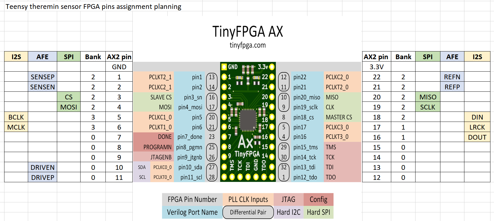
For FPGA main device, we can use any protocol we can imagine.

For MCU, some standard one, like SPI, I2C, I2S, is preferred since it has hardware support, and would not consume a lot of CPU resources.

Moving functionality off of the main FPGA would require some thought as to timing and synchronization.  When you've got a single clock inside a single FPGA everything can be fairly straightforward (if you have enough internal PLLs).

There are two parts of sensor to main board interface: configuration and realtime axis data.
Configuration includes FPGA configuration (bitstream) programming, and sensor parameters - like min/max freq range for PLL, scaling / linearizing parameters, etc. during calibration
Configuration parameters are rarely changed, and slow interface would work ok.
Realtime interface should be fast enough, and consume as little CPU as possible.
For each audio frame (e.g. once per 600 samples) we should poll axis values from two sensors.
SPI or I2C is probably ok, but I'm looking for I2S stream.
There is I2S audio input mostly useless in theremin. We can stream axis values one per sample, and they would be read by MCU using DMA.
I saw example of Maxh XO2 configuration update via I2C, so probably for calibration params it might work as well.
Not sure if two XO2 can share the same I2C interface. Is it possible to assign address?

For relatively low rate I2S bit clock (like 768KHz) it's easy to resolve all synchronization issues.

It makes sense to clock XO FPGA from external clock - e.g. from MCLK (~12.288MHz) signal of I2S - generated by MCU audio interface.
SysClock PLL of XO2 would generate all necessary internal clocks.

I'm going to design sensor with LVDS interfacing between DPLL FPGA and analog front end - in hope that it can reduce noise.
As well, we can use separate regulators - for FPGA, AFE, and even drive and sensing parts of AFE.


Vadim, the world seems to be crying out for a solid, full-featured, inexpensive Theremin, which you and I know is clearly doable with current technology.  I think FPGA-based LC DPLLs coupled to a cheap multi-core processor, with a touchscreen rather than encoders, might be the best way to go.  I hate to lash anything to the shifting sands of consumer computational solutions, but a cheap 7" tablet running an app comes to mind (otherwise one is re-inventing the wheel to some degree - though often that wheel could use some re-inventing, if only for increased control).  I'd really like to contribute to such a project, I'd certainly be up for porting all of my D-Lev code to it.

It would be great if you joined this project. You already contributes a lot by oscillators and sensors discussions.

Now I like Teensy based theremin idea - with tiny FPGAs for sensors. Using of FPGA DPLL sensors can eliminate the reason for main FPGA device.
iMXRT ARM core at 1GHz with ~1.5 instructions per cycle and using of tightly coupled memory (2 ports - instruction + data at the same cycle, or reading of two instructions w/o cache delays) exceeds D-Lev systhesizer power and gives a lot of space for experiments.
I believe D-lev synthesizer may be easy ported from HIVE ASM to C. Some of presets like human voices are really awesome.
GUI/controls - not a problem when programming in C/C++.
Teensy can execute one floating point instruction per cycle (with 4-byte float). Can we benefit from FP in some DSP algorithms?
LCD touch is pretty useful IMHO. Usual tablet most likely has capacitive touch and will suffer from 500Vpp antennas nearby.
Connecting of LCD with internal resistive touch and display SPI interface controllers seems ok for me.
2.8 or 3.2inch screens offered for teensy are probably good.
Anyway, I'm planning to have several encoders and pots, just in case - sometimes hardware controls are better than touch interface.

Posted: 11/19/2021 8:58:00 PM
dewster

From: Northern NJ, USA

Joined: 2/17/2012

"It would be great if you joined this project. You already contributes a lot by oscillators and sensors discussions."  - Buggins

Thanks!  It's fun and you keep me on my toes.

"Now I like Teensy based theremin idea - with tiny FPGAs for sensors. Using of FPGA DPLL sensors can eliminate the reason for main FPGA device."

I'm wondering if the Teensy processor along with a single FPGA might be the best solution?  That way the FPGA could send the data back at 48KHz via a single i2S link as you suggest, normally L & R stereo PCM data could instead be filtered 32 bit pitch and volume axis data?  As you also suggest, a high speed I2S clock could clock the FPGA logic (after some internal PLL multiplication) which might benefit from a differential connection.

If ESD can be addressed, it might be possible to connect the FPGA pins to the LC DPLL drive, in phase, and quadrature, rather than using an AFE, which could simplify things.  Then again, I like having sacrificial logic between the FPGA and the environment whenever possible.

So maybe a smallish FPGA with AFE circuitry on the same board, to the left and right?  The coils would give even more space between the antennas.

"I believe D-lev synthesizer may be easy ported from HIVE ASM to C. Some of presets like human voices are really awesome."

I use a lot of mixed (signed and unsigned) adds and multiplications that Hive directly supports, along with unsigned limiting and signed saturation.  I'm wondering how hard this might be to transfer to the teensy processor via C.

"Teensy can execute one floating point instruction per cycle (with 4-byte float). Can we benefit from FP in some DSP algorithms?"

I've read that filters are generally best done with fixed point, and I believe that to be true.  No resolution is lost, particularly when the filter is set to a very low cutoff frequency where attenuation is high before the accumulation.

Other algorithms could be simpler in float, but once they're coded in fixed point assembly you might as well just transfer them.

"LCD touch is pretty useful IMHO. Usual tablet most likely has capacitive touch and will suffer from 500Vpp antennas nearby."

I'm not so sure.  I've seen tablets functioning very near Theremins, like Thomas Grillo's setups.  I just put my $35 7" Fire tablet right next to the pitch plate on my lab unit and it works fine playing solitaire.

"2.8 or 3.2inch screens offered for teensy are probably good."

That seems kinda small, particularly for us old folks with old eyes! ;-)

"Anyway, I'm planning to have several encoders and pots, just in case - sometimes hardware controls are better than touch interface."

I agree, though all the trouble I've had with encoders makes me hesitant to use them again in a high wear situation, and they are difficult to interface.  Pots are good for holding state through a power cycle, but not much else, and need to have some hysteresis applied.  So I'd opt for using the touchscreen as much as possible.  I realize it's hard to do up-front, but think about what the various screens will contain and how various adjustments will be made, implement any physical controls around that, with an eye towards minimizing the physical controls as much as possible. 

Ideally you would just have a touchscreen and a power switch, if you could somehow make that work.  Or, for instance, you could select a single control on the screen with your finger and then spin a single encoder to change it.  If you only have a single encoder you could perhaps buy one that is higher quality, though good luck with that, because I haven't had any.

Posted: 11/23/2021 5:00:38 PM
Buggins

From: Porto, Portugal

Joined: 3/16/2017


I'm wondering if the Teensy processor along with a single FPGA might be the best solution? 
That way the FPGA could send the data back at 48KHz via a single i2S link as you suggest,
normally L & R stereo PCM data could instead be filtered 32 bit pitch and volume axis data? 
As you also suggest, a high speed I2S clock could clock the FPGA logic
(after some internal PLL multiplication) which might benefit from a differential connection.


For clocking of FPGA, single ended 12.288 MHz MCLK clock input should be enough. Anyway, teensy does not provide differential output for MCLK.
It's not a problem to combine I2S data from two FPGAs if we used two wires. Each FPGA reads I2S data from input and replaces left or right channel of data.
Any of these I2S data lines may be connected to I2S data input.

DPLL FPGA implementation may be dumb: just DPLL publishing filtered frequency (period) value via I2S. DPLL needs some limits for min/max PLL frequency.
Limits may be just hardcoded in FPGA firmware. In this case, the only interface with MCU needed is I2S.
We can add configuration interface between MCU and FPGAs - SPI. For simple DPLL, it may set min / max period value.
Instead of dumb DPLL, we can put most of logic into FPGA. For pitch sensor - scaling, linearization, pitch correction - ending with phase value
for each audio sample. This will reduce MCU CPU load. For volume sensor, we can do scaling / linearization / additional volume effects - and provide resulting volume as multiplier in I2S channel.
For such clever DPLL, a set of configuration / calibration parameters should be accessible via SPI.

As well, it would be great if we managed to use SPI for FPGA firmware update from MCU.

If ESD can be addressed, it might be possible to connect the FPGA pins to the LC DPLL drive,
in phase, and quadrature, rather than using an AFE, which could simplify things. 
Then again, I like having sacrificial logic between the FPGA and the environment whenever possible.


Not sure if it's a good idea to expose FPGA pins under ESD. But of course it's possible.
XO2 has drive current settings, and may provide enough current for driving LC tank.

So maybe a smallish FPGA with AFE circuitry on the same board, to the left and right? 
The coils would give even more space between the antennas.

Looks like obvious solution. Left to right: antenna, volume coil, volume AFE, volume FPGA, MCU, Audio board, pitch FPGA, pitch AFE, pitch inductor, pitch antenna.
Long narrow box cabinet.

I use a lot of mixed (signed and unsigned) adds and multiplications that Hive directly supports,
along with unsigned limiting and signed saturation.  I'm wondering how hard this might be to transfer to the teensy processor via C.

I've read that filters are generally best done with fixed point, and I believe that to be true. 
No resolution is lost, particularly when the filter is set to a very low cutoff frequency
where attenuation is high before the accumulation.

Other algorithms could be simpler in float, but once they're coded in fixed point assembly you might as well
just transfer them.


In many cases, one HIVE instruction will be translated to 2-3 ARM instructions, but anyway, MCU performance should be enough.


I'm not so sure.  I've seen tablets functioning very near Theremins, like Thomas Grillo's setups. 
I just put my $35 7" Fire tablet right next to the pitch plate on my lab unit and it works fine playing solitaire.


That seems kinda small, particularly for us old folks with old eyes! ;-)

The more I try to find big touch LCD with SPI interface (prices are usually $50-$75), the more I like idea to use tablet for GUI and control.
A lot of logic may be extracted to tablet application.

At least, Teensy's serial over USB interface is available for android apps. It is enough for controlling of theremin.
As well it's possible to implement MIDI and USB audio device.
Tablet just must to have USB OTG port.
Theremin may even be powered from tablet USB connection. Can it reduce noise from power line?

I agree, though all the trouble I've had with encoders makes me hesitant to use them again in a high
wear situation, and they are difficult to interface. 
Pots are good for holding state through a power cycle, but not much else, and need to have some hysteresis
applied.  So I'd opt for using the touchscreen as much as possible. 
I realize it's hard to do up-front, but think about what the various screens will contain and how various
adjustments will be made, implement any physical controls around that,
with an eye towards minimizing the physical controls as much as possible.

Ideally you would just have a touchscreen and a power switch, if you could somehow make that work. 
Or, for instance, you could select a single control on the screen with your finger and then spin a
single encoder to change it. 
If you only have a single encoder you could perhaps buy one that is higher quality,
though good luck with that, because I haven't had any.

Economy from removing of LCD, encoders and pots allows to buy cheap android tablet
Now I'm going to move in this direction


Learning about lattice FPGAs. Downloaded Diamond.
Tried to implement clocks and I/O.

Mach XO2 PLL max output frequency: 400MHz
It makes sense to use clocks synchronous to audo clocks.
I'm planning to use PLL based on 12.228MHz I2S MCLK clock which will be generated by MCU.
Multiplies are 98.304, 196.608, and 393.216MHz.
We can use 393.216MHz as DDR clock, and 98.304MHz as main data processing clock.
It gives 786.432MHz I/O rate (sampling precision). Not 1200MHz of Xilinx OSERDES in series 7 FPGAs (which uses dual 90 degrees shifted clocks - 4 edges instead of 2 edges in lattice devices), but should be enough.

Now it's hard to order LCMXO2-1200HC-4SG32C, at least here in Russia.
It's out of stock at most of market places. I see them available on arrow.com site.

XO2-1200HC breakout, TinyFPGA AX2 board is out of stock, too. Finally found it on aliexpress, and ordered two pieces. They are expensive and delivery is surprisingly expensive: ~$100 for two boards with delivery to Russia.
As well, I've ordered lattice programming cable from aliexpress (cheap enough).

For prototyping, we can live with 2xAX2 and teensy audio board, and switch to soldered XO2-1200 and sgtl5000 qfn32 in "production".
As well, for prototyping it makes sense to make analog front end part on separate PCB - to allow experiments with different types of AFE.

Planning pin assignment, to check if qfn32 xo2-1200 fpga is enough.


Code:
I2S interface:

MCLK      I2S master clock input
BCLK      I2S bit clock input
LRCK      I2S left/right clock input
DIN        I2S data input
DOUT      I2S data output

Sensor interface:

DRIVEP    diff lvds drive signal output, positive
DRIVEN    diff lvds drive signal output, negative
REFP      diff lvds reference signal input, positive
REFN      diff lvds reference signal input, negative
SENSEP    diff lvds sensing signal input, positive
SENSEN    diff lvds sensing signal input, negative

SPI interface:

CLK        hard SPI clock
SLAVE_CS  hard SPI select
MISO      hard SPI data output
MOSI      hard SPI data input

Pins assignment for TinyFpga AX2 board:


Started implementation in verilog.

Figured out that qfn32 device has only C and D I/O with limited functionality. No real LVDS drivers (which are available only in A and B I/O).
Input/output gearboxes (serializers/deserializers) probably missing too.
Implemented x8 serializer and deserializer using usual logic slices. Anyway, performance is the same as with gearboxes.
Top level module has MCLK clock input, PLL producing 3 clocks: DDR, DDR/2, DDR/4 (processing).
There are two deserializers - on inputs from AFE, and one serializer to drive AFE.
I/O standard for AFE interface is set to LVCMOS33D - differential cmos - instead of LVDS I was planning in the beginning.

Planned clocks, based on XO2 maximum ratings from documentation:

Code:
//              abs max    / grade  -6      -5      -4
// DDR clock:    786.432MHz      761.856  638.976  516.096
wire clk_400; // 393.216MHz      380.928  319.488  258.048
wire clk_200; // 196.608MHz      190.464  159.744  129.024
wire clk_100; //  98.304MHz      95.232  79.872  64.512

So, for -4 grade of AX2 board, DDR (sensor sampling) frequency is 516MHz.
Currently, values from MAX column are specified in project.
By some unknown reason timings analysis during synthesis does not complain about timings violations. Does it mean -4 grade device may sample with 786MHz rate?
BTW, what is sampling rate of D-LEV DPLL?

Diamond project is available on github.

Posted: 11/25/2021 2:31:21 PM
Buggins

From: Porto, Portugal

Joined: 3/16/2017

My orders for both TinyFPGA AX2 and LCMXO2-1200HC-4SG32C were cancelled - out of stock.
No chance to buy lattice FPGAs. Disappeared from arrow.com as well.
Next availability date for ICs - April/May 2022.
Semiconductor industry crysis?

Fortunately, there is cheneese FPGA manufacturer Gowin with GW1N series with many devices pin-to-pin compatible to lattice mach xo2 ones.
At least, there are some in stock, e.g. on mouser.com
Comparable devices, GW1N-LV1QN48C6/I5 and GW1N-LV1QN32C6/I5 are in-stock on Mouser, and cost ~$12 for one piece.
Actually, Lichee Tang Nano on GW1N-LV1QN32C6/I5 is available for $5 on aliexpress and amazon so it should be possible to buy these FPGA chips at lower price than $12.
Pin compatible gw1n-uv4qn48c6 is a bit expensive ($29), but has resources (4608 LUTs, 16 multipliers) for any crazy sensor ideas.

I've downloaded Gowin IDE, and tried it. Pretty similar to Diamond. Requires requesting of license (locked on MAC address of your PC).
IDE looks usable. Documentation in English is good enough.

Besides 1K (~lattice 1200), bigger GW1N FPGAs (2k, 4k LUTs) are available in the same packages.
Low voltage (1.2V core) version GW1N-LV1 is even faster than lattice HC1200 (884MHz sampling rate in gw1n-lv vs 645MHz of lattice HC).
High speed (3.3V core) version GW1N-UV gives 983MHz sampling rate, but UV is available for bigger FPGAs only - 2k, 4k...
As well, GW1N UV have true LVDS drivers. LV - do not. But we can use LVCMOS33D if we want differential I/O.
In both LV and UV, I've managed to use gw1n hardware IDES / OSER x8 serializers / deserializers.


I'm continuing pin planning, and FPGA code prototyping.

Nice to have ability - allow programming of both FPGAs from MCU.
It requires SPI Slave interface connection, with corresponding boot mode setting using pins.

I've checked

Boot modes are selected by MODE[2:0] pins. If some signal is not bound to pin, it's assumed as 0.

qfn32 devices:
Only mode[1] is available on pin: which gives two choices:
000: AUTO BOOT (from internal flash) and
010: MSPI when FPGA reads configuratoin from external flash or other devices via SPI as master.

qfn48 devices:
MODE[0] and MODE[1] are available, so it's possible to specify MODE=001 SSPI - programmable via slave SPI interface.

So, although qfn32 has enough pins for interfacing with both sensor AFE (1 diff out, 2 diff inputs), and MCU (enough pins for SPI and I2C), but it does not allow to use FPGA configuration upload via slave SPI.

Hmm... gw1n-uv4qn48c6 does not have MODE[0] pin... Ok. LV1 is probably enough.


Posted: 11/29/2021 2:06:21 PM
dewster

From: Northern NJ, USA

Joined: 2/17/2012

"Semiconductor industry crysis?"  - Buggins

It seems that way.  I wish I'd upgraded my PC before Covid hit.

"Actually, Lichee Tang Nano on GW1N-LV1QN32C6/I5 is available for $5 on aliexpress and amazon so it should be possible to buy these FPGA chips at lower price than $12."

Someone a couple of years back told me they could get the Cyclone FPGA I'm using for like ~$1 IIRC, which I find a little hard to believe because I was privy to the bulk pricing we could get where I used to work, but I guess you never know.

"I've downloaded Gowin IDE, and tried it. Pretty similar to Diamond. Requires requesting of license (locked on MAC address of your PC).  IDE looks usable. Documentation in English is good enough."

FPGA manufacturers invest huge amounts of time & effort & $ in SW tooling, and modern management best practices dictates they somehow turn this into a separate cost center - hence locked licenses, automatically expiring licenses, tiered tooling with a bare bones "freebie" targeting the very low end, etc. which ties the engineer's hands and creates extra busy work.  But of course the FPGAs are worthless without good tooling SW.  They're actually kind of worthless without fantastic SW!  FPGAs live and die by their SW and it's idiotic IMO to put up any barriers here.  If they were smart they would make it open source, but corporate secrecy must be observed above all else.  Altera and Xilinx were suing each other into oblivion in patent court until they called a truce.

"Nice to have ability - allow programming of both FPGAs from MCU."

That does make it easier to sleep at night, knowing the FPGA load can be part of your SW load.

Posted: 11/30/2021 1:36:34 PM
Buggins

From: Porto, Portugal

Joined: 3/16/2017


If they were smart they would make it open source, but corporate secrecy must be observed above all else.  Altera and Xilinx were suing each other into oblivion in patent court until they called a truce.

It looks strange for me, too. Free development tools + cheap small dev boards can give manufacturer wide base of experienced developers.

Lattice is the only FPGA manufacturer with available open source toolchain. Although, AFAIK, it's based reverse engineering, w/o Lattice help. At least they don't sue developers...


That does make it easier to sleep at night, knowing the FPGA load can be part of your SW load.

Flashing just single firmware update to MCU board, w/o additional two updates of FPGA using bulk chineese software seems like a big advantage.
MCU will program both FPGAs (upload two bitstreams via spi) in one second.

On Tang Nano boards, MODE0 and MODE1 are connected to GND via 4.7K resistors. Not available on pin.
To use SPI Slave programmin, MODE0 should be set to 1 - I hope it's possible to unsolder R, or solder wire to MODE0 pin.

Ordered a pair of tang nano.

BTW, it looks like nice breakout board for gw1n-1qn48 chip. Wondering if we can utilize 8MB PSRAM soldered on this board.
Place reverb/delay like effects into FPGA?
Started working on theremin PCB with teensy 4 + audio adaptor board + 2 x tang nano boards + 2 x sensor boards.

Posted: 3/14/2023 6:58:48 PM
Buggins

From: Porto, Portugal

Joined: 3/16/2017

I've designed yet another wallin oscillator.

LTSpice model can be downloaded from github.

BJT only version, powered from 3.3V (sources 12mA from power rail), for 2.7mH 120 Ohm R_serial inductor (air core with 0.1mm wire) it generates nice sine-like 1.35V drive signal, 3.7mA tank current with 150Vpp on antenna.
Phase error (delay between LC tank current and generated drive signal) is very small (10-15ns for 1MHz).
For inductors with lower R_serial it can give higher voltage swing.


Why current sensing (wallin oscillator)? I hope it receives less noise from antenna because one-side connected LC tank acts as a filter.
Why power rails sensing (dual shunt resistors vs single shunt resistor on output)? It can produce zero common mode signal. It's easier to design amplifier for such signal.
Why differential cascade is used? Previously, I've tried current mirror based current sensing on both power rails. But current mirror sensor gives big phase error when working in saturation mode. Properly tuned differential cascade produces smooth output when overloaded, without significant phase error.

Q5, Q6, Q7, Q8 form output buffer proposed by Eric.
Current through output stage Q7, Q8 is being sensed using R1, R2 shunt resistors (converted to voltage), C1/C2 divider gives voltage corresponding to difference between current flowing through upper and lower sensing resistors - which is equal to the current flowing through LC tank.
Using of capacitive divider C1/C2 allows to shift signal to point better suitable as amplifier input.
Differential cascade Q1, Q2 compares sensed voltage with constant bias point, and may produce output in range 1.4..3.3V
Q3, Q4 current mirror is to provide current source for differential cascade.
Q10, Q11 just an emitter follower to shift differential cascade output down by 0.7V to center it before passing to output buffer.

Drive voltage and LC tank current:


Antenna voltage swing:

Differential cascade symmetric outputs and drive signal after buffer.

6 BJTs may be replaced with single opamp. Opamp can give higher drive voltage swing - closer to power rails.
Schematic may be optimized to consume less power. But I'm afraid phase error may increase.
Changing of R1, R2 allow to tune "overload" of drive signal - choose between almost sine and something between sine and smoothed square.

I didn't try it on a breadboard. Not sure how would it react on hand touching antenna. Probably, oscillation would stop.


Posted: 3/17/2023 4:15:01 PM
Buggins

From: Porto, Portugal

Joined: 3/16/2017

Yet another wallin oscillator (github link to ltspice model).

Uses differential cascade with current mirror load - on 6 BJTs. This type of cascade provides current output.
Diff amp measures difference between currents flowing through top and bottom power rails of output cascade.
Due to current nature of output, drive voltage looks very strange, but I believe it's working good.
Powered from 3.3V, drives 120 Ohm inductor with 6.7mA 2.4Vpp signal giving 260Vpp voltage swing on antenna.
Consumes about 21mA from power source in this mode.
I believe phase error of this schematic is very small.


Inductor current and antenna voltage:


Differential cascade Q1, Q2 emitter currents and LC tank current:

Drive voltage and current:


Posted: 3/18/2023 3:57:51 AM
Yngvox Moogsteen

From: The Middle

Joined: 9/23/2021

Very interesting topic.  I would have viewed it sooner but it sounded like a law firm with a lot of partners......

Thanks 

Posted: 3/18/2023 2:32:41 PM
dewster

From: Northern NJ, USA

Joined: 2/17/2012

Vadim, thank you for posting your fascinating findings and sims!  I'm a bit underwater at the moment but plan to play with your designs shortly.  Your inverter version is the one to beat, truly an outstanding oscillator!

You must be logged in to post a reply. Please log in or register for a new account.