Let's design and build cool (but expensive) FPGA based theremin

Posted: 10/20/2022 5:57:20 PM
Buggins

From: Porto, Portugal

Joined: 3/16/2017


I found signed saturation and unsigned limiting to be extremely valuable, to the point where it needed to be done in processor HW for speed and economy.  In the end I used the extra BRAM bits they give you for ECC and such to hold flags that could then be decoded by the final mux to provide min/max.  This is from my multiply / shift / rotate unit:

It's really interesting idea for loading of unused 4 bits of BRAM with something useful.
I was thinking about increasing of instruction and data length by 2 or 4 ECC bits. But for memory, it can be used only if memory size is 2-4BRAM (depending on platform).
But since register file BRAM is small anyway, ECC bits are available.
Do you support byte-precise addressing and unaligned data in hieve?

BTW, I don't have stack support in my softcore architecture. Return address is saved to any register, and jump to value from any register may work as return (or even conditional return).
I'm avoiding stack instructions because POP instruction cannot follow rule "one instruction per cycle, only one register may be written per cycle". Pop requires saving of value from memory to register and save incremented/decremented stack pointer value.
Instead of incrementing/decrementing stack pointer on each pop/push, we can update it once per procedure call to reserve stack frame, and then address procedure parameters and local variables by addressing relative to stack frame pointer register.
When relation between procedure calls (call tree) is known, and if we have a lot of registers, we may assign non-overlapping registers as link registers for different procedures.

It took me a long time to come around to the fact that byte addressing is super valuable, and that variable length instructions - which is enabled by byte addressing - is also super valuable.  It's true that there are potential sync issues: you have to go back to the beginning and travel to the execution point to really know what the opcode is, but it's more than offset by the advantages IMO.

Hmm. Doesn't it require additional cycles if you support non-word aligned reads/writes and variable length instructions - it may take omre than one cycle to read instruction.
If prefetch is used - more than one cyle may be required on conditional jumps.


Meanwhile, I'm trying to find suitable FPGA board / module to use in digital theremin.


Found very interesting devices from german manufacturer Trenz Electronics: TE0725.

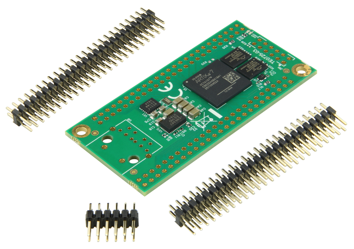
It's small Artix-7 based easy to solder board.
Power supply is 3.3V.
Status is Full Production, but it's not in stock. "Possible to order, delivery time on request."
Dual 2x25 easy to solder 100mil headers. Each of them supports has support 42 single ended or 21 LVDS pairs.
Each header is connected to its own HR I/O bank (bank 34, bank 35), and can have its own I/O voltage (3.3V from onboard regulator or other voltage from external supply).
E.g. one of headers may be powered from 2.5V (requires external regulator) providing full LVDS support, and outputs with voltage 2.5V can be connected to inputs of 3.3V devices.
On board 32MB flash, 8MB HyperRAM.
JTAG header and serial interface for programming / debugging.
TE0790 JTAG programmer board may be used for USB JTAG+Serial

There are several configurations - with different Xilinx Artix-7 chips:
XC7A15T-1CSG324C  (10K LUT6, 20K FFs, 45 DSPs, 25 BRAM, 5 PLL) - EUR 69  - useless configuration - same price A35T, but less power, slower speed grade (-1 instead of -2)
XC7A35T-2CSG324C  (20K LUT6, 40K FFs, 90 DSPs, 50 BRAM, 5 PLL) - EUR 69  - looks like optimal
XC7A100T-2CSG324C (60K LUT6, 120K FFs, 240 DSPs, 135 BRAM, 6 PLL) - EUR 134 x3 times more power for x2 bigger price
LUT6 can often replace two smaller LUTs, with separate FF on each half.

Very nice, but...
Mouser reports expected manufacturing time as Summer 2023.

Only chineese boards may save us

Sipeed Tang Nano 4K with 8MB of embedded SDRAM and embedded ARM hardcore, 4K LUTs.    EUR 18
Sipeed Tang Nano 9K with 8MB of embedded SDRAM, 8K LUTs       EUR 20  
Sipeed Tang Primer 20K, with 20K LUTs and big on-board SDRAM  EUR 28

QMTECH ZYJZGW Xilinx Zynq7000 Zynq XC7Z010 SoC FPGA Starter Kit Development Board on aliexpress for EUR 66
I believe it's not the same board as mentioned by Joel as having decoupling issues - link from Joel's list is outdated, and as I remember, it was different layout.

What about x10 times more LUTs, 300K?
QMTECH Xilinx FPGA Kintex7 Kintex-7 XC7K325T DDR3 Core Board from aliexpress    EUR 133
x30 times more resources than D-Lev currently have.
Unfortunately, it's not supported by free version of Vivado (up to Kintex XC7K160T only)

Ok, here is 200K LUT board
QMTECH Xilinx FPGA Artix7 Artix-7 XC7A200T DDR3 Core Board  on aliexpress EUR 133
But this one is supported - is biggest Artix chip supported for free.
Any crazy idea should fit.

These boards may disappear from market at any time.


Is there something suitable non-chinese in stock from brands?

Z-Turn Board
MYS-7Z020-C-S  mouser: 11 in stock EUR 175.5
Good but expensive Zynq 7010 board, with 50mil pin sockets below.
(or it's chinese, too?)

Cmod A7 Artix-7 Module: In stock everywhere. Farnell price EUR 87
DIP form factor with 44 digital I/O pins and 2 analog input pins, powerful 35K LUTs FPGA, but only 512K of external SRAM chip.


Posted: 10/20/2022 11:13:35 PM
dewster

From: Northern NJ, USA

Joined: 2/17/2012

Vadim, if you're interested I stuck my opcodes in a spreadsheet here: https://d-lev.com/support/hive_opcodes_2022-10-20.ods

The decode is fairly orthogonal, which helps to speed it up.  There are 1, 2, 3, and 4 byte instructions, and the lit instructions use the data port of the BRAM rather than the opcode port to give 8, 16, and 32 bit data.  Using dual port BRAM as main memory lets you do this, and it's quite convenient.

"It's really interesting idea for loading of unused 4 bits of BRAM with something useful."  - Buggins

Another notion I resisted for a long time because I thought it prevented the stacks from spilling into external RAM (where the flags would get stripped off) but the stacks are deep enough (32 entries) to not worry about filling them, something I didn't realize until I really started to program Hive in earnest.  I don't use the spare bits in main BRAM though, just for the stacks.

"BTW, I don't have stack support in my softcore architecture. Return address is saved to any register, and jump to value from any register may work as return (or even conditional return)."

I like that approach.  Hive has return stack support because it does as you do, but the 8 data registers are actually 8 stacks.  But due to stack coherence needs it can't do conditional return (it would have to do a conditional pop too, which I decided against as it seemed a bit tricky, and it wouldn't get used much anyway).

"Hmm. Doesn't it require additional cycles if you support non-word aligned reads/writes and variable length instructions - it may take omre than one cycle to read instruction."

The opcode port is 32 bits wide, with the opcode byte itself in [7:0], usually followed A&B stacks select and pop in [15:8], followed by one or two bytes of immediate data above this.  If an operation is e.g. 1 byte, the next fetch is to PC++; 2 bytes PC+=2, etc. so redundant bytes are often read and ignored, but there is no need to capitalize on that in any way.

"Meanwhile, I'm trying to find suitable FPGA board / module to use in digital theremin."

Wow!  Thank you for those links, great stuff!

"But this one is supported - is biggest Artix chip supported for free.  Any crazy idea should fit."

I worry about current draw, particularly via USB, as well as heating.  Right now Hive is pulling ~0.5A or 2.5W, which is right at the edge of allowable via the USB spec.  A real processor would likely draw quite a bit less while running rings around Hive.  USB electrical interfaces come and go, but they guarantee a certain voltage and correct phase, and it keeps me from having to deal with all the AC systems in the world.

"Very nice, but... Mouser reports expected manufacturing time as Summer 2023."

I wonder if it's time to just hunker down and do more R&D and documentation?  Waiting for the world to change...

Posted: 10/29/2022 9:09:23 PM
Buggins

From: Porto, Portugal

Joined: 3/16/2017

In this post I will describe my investigation of possible maximum performance of theremin sensors and barrel CPU softcore achievable for Xilinx Series 7 speed grade -1 FPGA.
(assuming we need to use clocks synchronous to audio sampling clock 48KHz)
As well, I have an idea about reducing of sensor I/O aliasing.


Let's try to estimate clocking for digital theremin based on Xilinx Artix (Series 7) FPGA. For Zynq, FPGA part is the same as Artix.
Assuming available external clock is 100MHz (xtal on most of available boards).
Speed grade of available boards is usually -1 (with -2, higher frequencies are achievable).

Theremin sensor is based on Eric's (dewster) approach, DPLL with current sensing.

Sensor will be implemented using FPGA-side digital PLL approach. Sensor DPLL will generate DRIVE output frequency passed to Analog Front End (AFE) via either single ended or differential LVDS connection.
AFE will feed LC tank (L = coil, C = antenna capacity) with this signal and return back to FPGA two signals: REF (feedback - copy of DRIVE signal) and SENSE - phase shifted signal from LC tank.
REF and SENSE signals may be transmitted either via single ended LVCMOS33 or differential LVDS lines.
Current sensing method (measure of current flowing through inductor) is planned to be used.
If DRIVE signal frequency is equal to LC tank resonant frequency, REF and SENSE will have zero phase shift (for current sensing approach).
When DRIVE frequency is lower or higher, phase shift between REF and SENSE signals appears. DPLL will measure phase shift and use this value to correct DRIVE signal frequency.

For generation of DRIVE signal, we can use NCO (numerically controlled oscillator) with DDR output.
OSERDESE2 primitive in 4:1 DDR mode will be used to achieve maximum resolution of NCO. In this mode, OSERDESE2 needs two clocks: source data clock to feed serializer with 4 bits of data per clock cycle, and one DDR clock with x2 higher frequency which would shift bits to output on each raising and falling edge of DDR clock.

For measuring of REF and SENSE signals phase shift, we can use deserializer on ISERDESE2 in either DDR or OVERSAMPLING mode.
In DDR 4:1 mode, input serializer samples input twice on both edges of DDR clock and provides 4-bit output of deserialized sample data. Clocking is similar to OSERDES, but it requires two DDR clocks - normal and inverted.
As well, I'm going to try implementing Oversampling mode 8:1 on ISERDES. In this mode, 4 phases of DDR clock should be provided (0, 90, 180, 270 degrees).
Oversampling ISERDES will provide 8 bits of deserialized data once per CLK cycle. REF and SENSE signals in oversampling mode will be sampled with x2 higher rate than in DDR mode.

It's planned to use 8-threaded 32-bit Barrel Processor softcore to handle sensors, synthesize sound, and do a lot of configuration and UI stuff.
With barrel processor approach, CPU pipeline clocked at CLK frequency will execute 8 threads sequencially each in different pipeline stage.
Effective clock for single thread is 1/8 of CLK, CLK_DIV8.
DDR clock for I/O will have frequency CLK*2, CLK_MUL2.
Sampling rate of sensor I/O in DDR mode is CLK*4.
Sampling rate of sensir inputs in Oversampling mode will be CLK*8.

It makes sense to have all clocks synchronized with Audio clock (48KHz). With barrel processor, let's make CLK_DIV8 to be multiply of audio clock.
In this case, CPU will execute integer number of instructions per one audio sample. As well, it will simplify noise filtering.

NOTE: although REF signal (DRIVE feedback) is just const-time delayed version of DRIVE, and can just be replaced with constant shift of DRIVE internally in FPGA, in real world this delay may vary, depending of components, environment temperature, etc.
So, we still need to measure REF signal. But if sample REF input with the same clock as DRIVE, it will be highly aliased to DRIVE, and we cannot measure its exact value.
To minimize REF signal measurement aliasing, we can use separate clocks for sensor inputs with different frequencies - it will give us dithering, allowing to know positoin of REF signal with higher precision.
Let's plan to use separate clocks for sensor inputs. Measured phase shift value should be passed to main processing clock domain. But it's not a problem, since we only get new value of phase shift at edge of signal - twice per DRIVE signal period (a few MHz).
After conversion to main clock domain, phase shift data may be filtered to eliminate steps and influence of domain crossing noise.
If input I/O clocks are still multiplies of audio clock, noise of clock domain crossing will be filtered out completely.


To plan clocking, we need to know FPGA frequency limitations.

I've extracted some max frequency information from Artix datasheet.

Code:
Primitive          Max frequency, MHz             Description
            Speed grade -2  grade -1
----------  --------------  ---------    -----------------------------------------
BUFG                   628        464    Global clock buffer
BUFR                   375        315    Regional clock buffer
DDR LVDS              1250        950    OSERDES with DDR LVDS transmitter
2:1 DDR3               700        620    DDR3 memory IP maximum PHY interface rate
4:1 DDR3               800        800    DDR3 memory IP maximum PHY interface rate
BRAM RF DW             404        339    Block memory, Read first, possibility to address overlap on two ports
BRAM RD DW CAS         365        297    Block Memory, Cascading mode, read first, possibility to address overlap on two ports
DSP ALL REGS           550        464    DSP fully pipelined, no pattern detection
DSP ALL REGS PATDET    465        392    DSP fully pipelined, with detection
DSP MUL NOMREG         305        257    DSP MUL w/o MREG, no pattern detection
DSP MUL NOMREG PATDET  277        233    DSP MUL w/o MREG, with detection

From table above, we can see that main limiting factor of clock frequencies is BUFG (global clock buffer).
BUFG max frequency of 464 MHz will limit possible I/O SERDES clocking.
It will lead to 232MHz main data processing CLK, which is far below other limits.
But actually it's not bad. E.g. DSP block working at lower frequency may be configured with less pipeline stages - giving 1 cycle less pipeline latency.
As well, lower clock reduces design limitations (e.g. number of LUT layers, fabric connection distance, fanout) - no need to use tricks to bypass violations found by static clock analysis.


Another limitations may come from FPGA clocking primitives and real source (xtal) clock frequency.

In Xilinx Series 7 FPGA, there are PLL and MMCM hardware blocks.
PLL can take source frequency FSRC, generate internal VCO frequency locked on FVCO=FSRC*VCOMUL/VCODIV, and then provide several output frequencies which are integer dividers of FVCO, with optional phase shift.
MMCM is just an advanced version of PLL - one of generated frequencies may have "fractional" divider.

Due to limitations of clocking primitives, only a limited set of output frequencies can be achieved.
After applying of 48KHz Audio Clock phase alignment constraint, and source clock frequency constraint, it's getting hard to produce a set of clocks close to max bound.

From 100MHz it's hard to generate set of clocks which are exact multiplies of 48KHz.
But we can add one more PLL to generate intermediate clock, which is more suitable for generation of multiplies of 48KHz.
I've found that 96MHz clock as PLL input allows to achieve better (closer to max bounds) clocking.

So, let's just use two PLLs: first will convert 100MHz on-board oscillator frequency to 96MHz, and second will produce set of CLK, CLK_MUL2, CLK_DIV8 - phase aligned with 48KHz, and close to max supported FPGA frequency.
First PLL can also be used to provide separate clocking domain for sensor inputs (to reduce aliasing).

For max sensitivity of sensor, and maximum performance of CPU, let's try to provide clocks close to max FPGA limits (464MHz for CLK_MUL2).


First stage of clocking: MMCM, for input deserializers and to feed second stage PLL
Input clock: 100MHz  PLL VCO frequency: 900MHz


Code:
Clock name     Frequency, MHz   Phase  Divider    Description
-------------  --------------   -----  -------    ---------------------------------------
CLK96                      96       0    9.375    Internal clock to feed second stage PLL
CLK2_MUL2                 450       0    2        ISERDESE2 oversampling mode shift clock
CLK2_MUL2_90              450      90    2        ISERDESE2 oversampling mode shift clock
CLK2_MUL2_180             450     180    2        ISERDESE2 oversampling mode shift clock
CLK2_MUL2_270             450     270    2        ISERDESE2 oversampling mode shift clock
CLK2                      225       0    2        ISERDESE2 output clock


Second stage of clocking: PLL, clock source for most of parts
Input clock: 96MHz    PLL VCO frequency: 921.6MHz

Code:
Clock name     Frequency, MHz   Phase  Divider    Description
-------------  --------------   -----  -------    ---------------------------------------
CLK_MUL2                460.8       0        2    OSERDESE2 DDR shift clock
CLK_MUL2B               460.8     180        2    OSERDESE2 DDR shift clock
CLK                     230.4       0        4    Main processing clock for most of modules
CLK_DIV8                 28.8       0       32    CLK/8: Single thread clock cycle


Selected frequencies give following performance metrics:

Code:
Input sampling rate, ISERDES 4:1 DDR mode:            900.0MHz
Input sampling rate, ISERDES 8:1 oversampling mode:  1800.0MHz
Output sampling rate, OSERDES 4:1 DDR mode:           921.6MHz
CPU and most of other processing frequency:           230.4MHz
CPU single thread frequency:                           28.8MHz


Clocks are multiples of CLK_AUDIO, 48KHz:

Code:
  CLK/CLK_AUDIO       =  230.4/0.048 = 4800
  CLK_DIV8/CLK_AUDIO  =  28.8/0.048  =  600
  CLK2_MUL2/CLK_AUDIO =  450/0.048   = 9375
  CLK_MUL2/CLK_AUDIO  =  460.8/0.048 = 9600


Input sampling rate and output sample rate clock domains relation:

Code:
  CLK_MUL4:CLK2_MUL4  =  921.6:1800  = 64:125

So, ISERDES (REF, SENSE) sampling phase will match phase with OSERDES (DRIVE) only once
per 125 input sampling clock cycles or once per 64 main processing clock cycles.
Phase combination will repeat at 1800/125=14.4MHz rate.
I hope it should give some dealiasing to REF phase position measurement.

What I've tested in Vivado implementation timing simulation:
- Clock generation
- Input deserialization in DDR 4:1 mode (in CLK clock domain)
- Output serialization in DDR 4:1 mode
- Checked OSERDES-ISERDES-OSERDES chain to ensure waveworms are preserved

Next things to be done:
- Implement oversampling mode input deserializer, and test in on simulation.
- Use CLK2 clock domain for input deserializers.


Posted: 10/30/2022 10:29:25 AM
dewster

From: Northern NJ, USA

Joined: 2/17/2012

"It makes sense to have all clocks synchronized with Audio clock (48KHz). With barrel processor, let's make CLK_DIV8 to be multiply of audio clock."  - Buggins

At one point I decoupled the core frequency from everything else, and I'm glad I did as it allowed me to lower it from 200MHz to 180MHz.  As more and more peripheral logic started packing in, seed search synthesis started taking forever.  Even 180MHz is kinda pushing it, to the point where I'm rather disinclined to update the FPGA load very often (other than to update the BRAM boot code, which doesn't require re-synthesis).

"So, we still need to measure REF signal. But if sample REF input with the same clock as DRIVE, it will be highly aliased to DRIVE, and we cannot measure its exact value.  To minimize REF signal measurement aliasing, we can use separate clocks for sensor inputs with different frequencies - it will give us dithering, allowing to know positoin of REF signal with higher precision."

A novel approach!  But IMHO this isn't an enormous deal as you have plenty of resolution.  Triangular dither applied to the drive side, with the exact same frequency as your  sampling rate, plus environmental noise (mostly mains hum), will give you very clean data to further LP and notch filter.  You reach a certain point and internal interference is probably more of a problem than resolution limitations.  Because of the strong influence of the human body, the very far field (the reason for high resolution) is essentially unplayable with ANY Theremin - luckily mathematically linearizing the very near field gives more range where the player has the most control - win/win (if you can persuade analog players to play there).

"From 100MHz it's hard to generate set of clocks which are exact multiplies of 48KHz.  But we can add one more PLL to generate intermediate clock, which is more suitable for generation of multiplies of 48KHz."

I had to use two PLLs to get close to 48kHz too from the 50MHz crystal (they should use something closer to a power of 2 here).  Not ideal, and actually at the limit of the SPDIF spec, but it works - particularly through a DAC box where all anyone sees is analog on the other side.

Posted: 11/7/2022 4:28:37 PM
Buggins

From: Porto, Portugal

Joined: 3/16/2017

Found TE0725-03-35-2C  47 In Stock on digikey.


But it costs EUR 121 with VAT - more than on Trenz site (EUR 82, but not in stock).
Most likely, I'll order it next week.

Artix XC7A35T FPGA has 20K LUTs, 40K FFs, 90 DSPs, 50 BRAMs(2700 Kbits)
It's "-2" speed grade FPGA - supports higher frequencies than "-1"
There are cheaper -1 grade boards with the same pinout (of course, not in stock).
Two 50-pin headers with 2.54mm pitch, provide 42+42 I/O pins.
Powered by 3.3V external supply. On-board regulators are linear ones.

It's possible to supply IO bank voltage for each connector (requires unsoldering of R0 resistor(s) on board).
With 2.5V supply on one of banks, we can use LVDS differential interface on this bank, still having the ability for 2.5V outputs to interface with 3.3V inputs in peripherial devices.
E.g. I'm planning to use 2.5V outputs to connect 3.3V RGB interface LCD.
If 20K of LUT6 is not enough, 100T boards (60K LUT6) with the same pinout may be used in project once get available.


At one point I decoupled the core frequency from everything else, and I'm glad I did as it allowed me to lower it from 200MHz to 180MHz.  As more and more peripheral logic started packing in, seed search synthesis started taking forever.  Even 180MHz is kinda pushing it, to the point where I'm rather disinclined to update the FPGA load very often (other than to update the BRAM boot code, which doesn't require re-synthesis).


I'll try to keep CPU core in sync with audio and sensors so far. But I can always separate them if core logic is getting too hard to support high clock frequency.


A novel approach!  But IMHO this isn't an enormous deal as you have plenty of resolution. 

Triangular dither applied to the drive side, with the exact same frequency as your  sampling rate, plus environmental noise (mostly mains hum), will give you very clean data to further LP and notch filter.  You reach a certain point and internal interference is probably more of a problem than resolution limitations.  Because of the strong influence of the human body, the very far field (the reason for high resolution) is essentially unplayable with ANY Theremin - luckily mathematically linearizing the very near field gives more range where the player has the most control - win/win (if you can persuade analog players to play there).

Now I'm trying to get as much as possible sensitivity from sensor.
LVDS differential connection of sensor AFE is probably overkill, but I'd like to keep the ability to experiment with it.
Differential I/O should significally reduce noise from I/O power supply, and noise from transmission lines.
I believe, current sensing approach should be more noise immune because antenna is isolated from sensing cirquit by large L inductor.
Eric, didn't you try to replace standard D-Lev AFE with current sensing cirquit?
With lower noise level, additional 1-2 bits in sensor I/O resolution may be visible.
Triangular 48KHz dither is planned, too.

I had to use two PLLs to get close to 48kHz too from the 50MHz crystal (they should use something closer to a power of 2 here).  Not ideal, and actually at the limit of the SPDIF spec, but it works - particularly through a DAC box where all anyone sees is analog on the other side.

Doesn't Altera PLL allow to generate exact 48KHz from 50/100MHz? Is it possible to get exact value using third PLL?

Posted: 11/8/2022 3:26:18 PM
dewster

From: Northern NJ, USA

Joined: 2/17/2012

"But it costs EUR 121 with VAT - more than on Trenz site (EUR 82, but not in stock).  Most likely, I'll order it next week."  - Buggins

You might contact Trenz directly to see if they really don't have any to sell?  Maybe explain your situation, forced to buy from a distributor for more $.

"It's possible to supply IO bank voltage for each connector (requires unsoldering of R0 resistor(s) on board)."

Hmm.  I wonder if using resistors here might impact signal integrity?  Might be best to route the supply pins directly to the power plane?  Probably a minor thing...

"With 2.5V supply on one of banks, we can use LVDS differential interface on this bank, still having the ability for 2.5V outputs to interface with 3.3V inputs in peripherial devices."

How about 3.3V inputs?

"I'll try to keep CPU core in sync with audio and sensors so far. But I can always separate them if core logic is getting too hard to support high clock frequency."

The way I handle sync is to have the DPLLs run at the SPDIF frequency (~200MHz) and snag the filtered frequencies at the interrupt rate of 48kHz, which gives the threads the entire IRQ period to go get the data.  This is an easy way to shuffle parallel data to the core clock domain without using gray codes and weird multi-domain timing constraints.

"I believe, current sensing approach should be more noise immune because antenna is isolated from sensing cirquit by large L inductor."

Ooh, I hadn't even thought of the low pass nature of the inductor!  But is it truly low pass if you're looking at the current through it?  I need to think about this more.

"Eric, didn't you try to replace standard D-Lev AFE with current sensing cirquit?"

No.  But I'm thinking more and more of trying your excellent hex inverter oscillator in a bench build.  It just works so well, and is quite stable, it could really simplify things in the system and with interconnect.  I need to do a spreadsheet to see if the same linearization method would work with period measurement rather than frequency measurement.  Of course you could just take the inverse first, but it might be best to do the subtraction (maths "heterodyning") as the very first step, like the D-Lev currently does.

"Doesn't Altera PLL allow to generate exact 48KHz from 50/100MHz? Is it possible to get exact value using third PLL?"

I thought I was cascading PLLs, but I'm not (the tool warns against this if you do as it can degrade absolute timing constraints):

50MHz * 18/5 = 180MHz core (processor & some peripherals) clock. 

50MHz * 59/15 = 196.666667 SPDIF clock.  This clock is supposed to be 48kHz * 2^12 = 196.608MHz, so the result is +298ppm, which is right at the edge of the SPDIF spec.

Posted: 11/8/2022 9:47:50 PM
Buggins

From: Porto, Portugal

Joined: 3/16/2017


You might contact Trenz directly to see if they really don't have any to sell?  Maybe explain your situation, forced to buy from a distributor for more $.

I've submitted my request in "contact us" form on Trenz site two weeks ago.
No response.

How about 3.3V inputs?

Artix pins are not tolerant to input signal voltage - it should not exceed bank supply voltage.
You cannot connect 3.3V external device output to 2.5V FPGA input.
But this signal may be read with 3.3V bank (another side of FPGA board).

2.5V bank output exceeds 3.3V middle point 1.65V so it should be ok to to connect 2.5V FPGA output to 3.3V external logic input.

Ooh, I hadn't even thought of the low pass nature of the inductor!  But is it truly low pass if you're looking at the current through it?  I need to think about this more.

BTW, can adding of some small cap on sensing side inductor reduce high frequency noise even more?
When I tried to experiment with current sensing oscillator, I still was able to see high enough noise, especially 50Hz main hum.
But I was using single ended oscillator to MCU connection, and this noise might be actually caused by power supply.
I wonder if LVDS with its comparator on input may significantly reduce power supply noise.


I need to do a spreadsheet to see if the same linearization method would work with period measurement rather than frequency measurement.


I believe, while difference of frequency for far and near hand distance is small (e.g. 5-7%), both frequency and period plot for this range are close enough to linear.
E.g. let we have 8% frequency change, 1MHz..1.08MHz for working range: 1.00, 1.01, 1.02, ... 1.08MHz
Period will be 1/f: 1.0, 0.9901, 0.9804, ... 0.9346 usec
Just try to add chart for both series in Excel. You will not notice difference between linearity of frequency and period, although frequency plot is straight line while period is not.
So, the same linearization method may be applied to both frequency and period.

Posted: 12/12/2022 7:51:42 PM
Buggins

From: Porto, Portugal

Joined: 3/16/2017

There is an interesting device mentioned in this post by Grumble.

AD9833 is a waveform generator which can generate sine wave with 25MHz sample rate and 10-bit DAC resolution.


It would allow to design clean sine wave driven oscillator. Can we get any advantage from pure sine driving?
Generator frequency (28-bit phase increment) may be updated via 3-wire SPI (with 25MHz SPI clock - with up to 750KHz rate).
While single chip costs $12, there are a lot of small boards available at lower price ($2.5..$3.5), with AD9833 and onboard xtal 25MHz.
Lifehack: buy board and unsolder the chip.
Even $12 price corresponds to preces of 8bit 100MHz DACs. There are a lot AD9833 in stock. Stock for DACs is much lower.
AD9833 has only 25MHz sample rate, but 10 bits resolution is avesome. DACs with 10bit resolution are expensive.
To control AD9833 you need only 3 wires (if CLK is the same for sampling and SPI). For DACs you would need 8 or 10 FPGA pins to implement the same waveform generation.
AD9833 output is only 0.038V..0.65V and should be scaled up (e.g. using opamp) to get higher voltage swing.

On my simulation, serial LC tank (for current sensing, one side of inductor is drive, another side of inductor is antenna) driven with 5V powered opamp AD8651 with 1K+6.2K resistors giving 0.4..4.6V sine drive via 10 Ohm, with 2.7mH inductor (120 Ohm serial resistance, 1.2pF self capacitance) and 8pF antenna gives ~500Vpp swing on antenna.

Analog front end with sine wave drive, current sensing and LVDS outputs would cost about $30 for ICs.

Code:
AD9833    1  EUR 12.68  waveform generator
AD8651ARZ 1  EUR  4.24  r/r opamp
ADCMP604  2  EUR  6.84  fast rail-to-rail comparator with LVDS output


Posted: 12/12/2022 8:47:18 PM
dewster

From: Northern NJ, USA

Joined: 2/17/2012

Sinewave drive gets you around the need for dither, but dither isn't that huge of a deal if you're doing it in an FPGA.  I found my first sticky spot the other day, and a bit of 48kHz triangular dither smoothed it right away (the default level is quite low).

Sinewave capture would be great, and would reduce potential aliasing at the squaring-up (done in the D-Lev AFE), too bad that isn't easy.

I keep thinking about fixed frequency drive with phase measurement of hand position.  This gives max. resolution in the far field, where the coil Q is providing a bunch of phase gain.  The ACAL process might then just set the oscillator frequency to give 90 degrees phase (or 0 degrees if sensed on the drive side) and then lock it.  The response would be fairly predictable but non-linear, not sure if my linearization method would fix it without another step of something else.

Lower voltage coil drive might make active shielding possible.

Posted: 12/12/2022 9:45:19 PM
Buggins

From: Porto, Portugal

Joined: 3/16/2017


Sinewave drive gets you around the need for dither, but dither isn't that huge of a deal if you're doing it in an FPGA.  I found my first sticky spot the other day, and a bit of 48kHz triangular dither smoothed it right away (the default level is quite low).

With AD9833, dithering is easy. Altering of phase increment can be applied at any time, and will be visible in waveform immediately.

Sinewave capture would be great, and would reduce potential aliasing at the squaring-up (done in the D-Lev AFE), too bad that isn't easy.

Do you mean, ADCs should be used for sensing? 2x8 or 2x10 bits for ADC input of drive and sense signals consume too many pins.
I believe, comparator based crossing zero (for drive) and current direction (for current sensing) should be enough.

I keep thinking about fixed frequency drive with phase measurement of hand position. 
This gives max. resolution in the far field, where the coil Q is providing a bunch of phase gain. 
The ACAL process might then just set the oscillator frequency to give 90 degrees phase (or 0 degrees if sensed on the drive side) and then lock it. 
The response would be fairly predictable but non-linear, not sure if my linearization method would fix it without another step of something else.


Proposed current sensing + AD9833 front end allows fixed pitch phase shift based implementation as well.
Last time I tried to simulate phase shift on LTSpice, collected data for C_hand to phase shift (or hand position to phase shift) values relation was similar to atan() as far as I remember.
I think, table based linear approximation approach may provide any linearization tuning you need.

Lower voltage coil drive might make active shielding possible.

Do you have any experimental proof that active shielding does work?

You must be logged in to post a reply. Please log in or register for a new account.