New Mixer Topology

Posted: 3/19/2013 1:03:05 AM
FredM

From: Eastleigh, Hampshire, U.K. ................................... Fred Mundell. ................................... Electronics Engineer. (Primarily Analogue) .. CV Synths 1974-1980 .. Theremin developer 2007 to present .. soon to be Developing / Trading as WaveCrafter.com . ...................................

Joined: 12/7/2007

I would have thought that, after my comments last time you distorted my words, you might refrain from doing so again! - Obviously I never made my annoyance at that dishonesty clear enough!

I NEVER SAID >> I have a design which uses a heterodyning ALU << I SAID >>Is like me saying "I have a design which uses a heterodyning ALU" <<

I would never bother wasting my time with heterodyning a ADC or (if possible, which I doubt) heterodyning a ALU..

What on earth is the point in having an ADC to do heterodyning for a digital system? All the disadvantages of having a fixed frequency digital  "reference" (the ADC clock) with a VFO "heterodyning" with it! (major disadvantage being that the thermal drift from the VFO will not be compensated by similar thermal drift from an analogue reference oscillator)

 - If you want to do things digitally, there are far simpler, cheaper and more reliable ways to get the VFO signal into the MCU / DSP to derive and process pitch data - See Dewsters Digital Theremin thread.

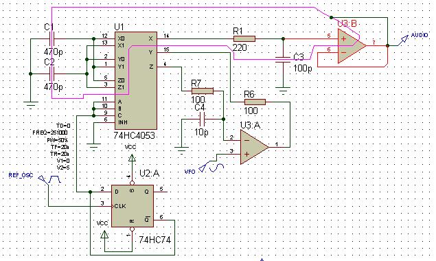
Just another needless layer of complexity when all you need to do is feed the VFO into the MCU / DSP, or if you do want to use "heterodyning" simply feed the reference clock into the CK input of a D Flip-Flop and the VFO into the D input of this FF, and get a clean tidy logic level square wave difference frequency out which you can process however you want.

Your "to reconcile a digital guy with analog girl" is quite funny - You are getting the worst of "analogue girl" and the worst of "digital guy" - You dont get a "true" analogue theremin waveform (the "analogue girl" needs an "analogue guy" - as in, one needs two analogue oscillators to get an analogue waveform which is the result of multiplying the oscillator waveforms and their harmonics .. and you also lose shaping which comes from the distortion of BOTH oscillators due to coupling).. and you gain no advantage in the digital implementation either.

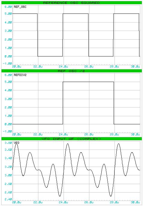
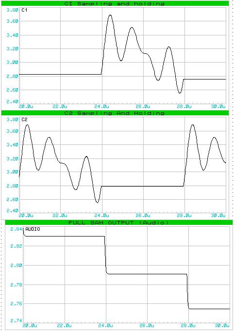
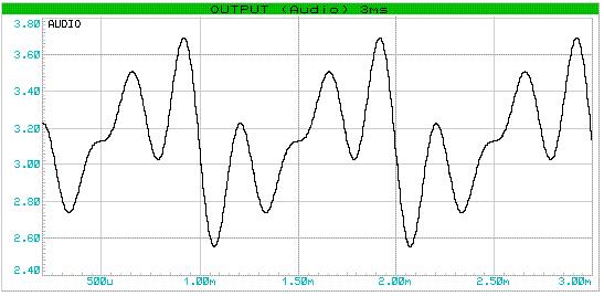
Now - IF your ADC were able to grab a sample quickly enough, then whatever waveform appeared on the VFO input would appear, at the difference frequency, on the output...

But hey - thats what I did! - and I didnt  need an ADC! - And I got slammed by you for producing a system far simpler and better than your half-baked idea! - And I published the idea in complete form, with full schematics and description and waveforms clearly and unambiguously in a way that anyone can follow and use and build! .. And I did this before anyone had ever even mentioned anything similar, let alone  published anything similar!.. So go chew on your sour grapes!

- I can have analogue oscillators which couple to each other if I wanted, square up the reference oscillator to drive the sampling, and grab the synced (distorted) VFO waveform.. On the sample 'playback' compress the waveform to achieve the identical effect of two oscillators being heterodyned..  But I also have total control of the waveform simply by changing the VFO shape.. And I can use analogue oscillators which track each other avoiding thermal drift problems, and produce whatever waveforms I want - "artificially" created, "naturally" created, or created by additive analogue synthesis...

And whats more, I have given ALL the data that is needed for ANY competent person to read and understand and use .. Its not just saying "I can do this - nah nah!" like some people here do >> "But there are ways..." << without disclosing those "ways".

I can supply high resolution pitch data which isnt subject to latency at low audio frequencies to any digital elements or pitch to voltage converters or whatever I choose.. Oooh - Sorry.. Havent disclosed that here for a long time.. But dont bother - Thierry declared that idea a waste of time so it must be a waste of time - even though I have a theremin pitch to voltage converter based on what I posted which can resolve frequencies down to 20Hz in under 7ms.

But Thierry and you and your kind have won! I aint going to post anything useful here any more - Its just not worth the bother.

"In general, there is nothing interesting here."

Your right! It would be interesting if I had not thought of sampling a theremins HF waveform to duplicate that waveform at the difference frequency based on the a sampling (reference oscillator) clock - But I did think of it!  And I published it here! And I did this before anyone else anywhere else even mentioned the idea!

How DARE you first lambast what I presented as "nothing new" then present the same concept in an innefficient form and try to say that what you have presented is worthy of any note!

Fred.

Posted: 3/19/2013 2:29:15 AM
Amethyste

From: In between the Pitch and Volume hand ~ New England

Joined: 12/17/2010

Ok everyone, get in line for "Hug Therapy"!!!

Who's the first? :)

Posted: 3/19/2013 2:43:32 AM
SewerPipe

From: Flying with the Phoenix

Joined: 3/9/2011

Amey; I haven't contributed in this thread at all, --but,---- Can I still have a "Hug"?? (-:

IHS ---- Dana


Posted: 3/21/2013 1:00:28 PM
Amethyste

From: In between the Pitch and Volume hand ~ New England

Joined: 12/17/2010

Anyone wating a hug (or many) is always welcome :) It's good therapy for the soul...

Posted: 3/28/2013 5:08:46 AM
FredM

From: Eastleigh, Hampshire, U.K. ................................... Fred Mundell. ................................... Electronics Engineer. (Primarily Analogue) .. CV Synths 1974-1980 .. Theremin developer 2007 to present .. soon to be Developing / Trading as WaveCrafter.com . ...................................

Joined: 12/7/2007


I think the above indicates that my circuit is not a mixer or multiplier..

The pulse of amplitude "1" (lets call this "REF") being narrow enough to provide equal amplitude harmonics which another signal (lets call this "VFO") can be multiplied with to produce a replication of this (VFO) waveform at the difference frequency, will have greatly reduced spectral amplitude..

For example, if a complex repetitive VFO waveform  is mixed / multiplied with the above (REF) pulse, each harmonic of the VFO waveform will be multiplied by about MINUS 38db.. (it should be easy to precisely compute the exact amplitude of harmonics from the pulse - but it makes little difference to the argument I think.. Even if only -18db, the argument still stands - there will be a big reduction in amplitude)

The whole VFO waveform could be reproduced (at the difference frequency), but its amplitude would be -38db after recovery..

With my circuit, it certainly appears that there is NO MULTIPLICATION - The amplitude of the output waveform is the same as the amplitude of the (VFO) input waveform.. The amplitude of the REF "pulse" waveform is unimportant provided it can drive the sampler.. Note also, the "pulse" does not actually exist - a 50:50 square wave at 1/2 the reference frequency drives a 2 part SAH, a "pulse" function could be envisioned as the change of state of this SAH, but this is the wrong way of thinking about things - its a sampler / SAH, not a multiplier!

With multiplication, both the sum and difference frequencies are produced, and  filtering is required to remove the sum components..

With my circuit, sum components are not produced - (more proof I think that this is not a multiplier or ring modulator) .. filtering is therefore not required.

From a perspective of "selling old wine" I am not doing myself any favours - People want "heterodyning" and are less keen I think on "sampling" - But the huge advantages of my circuit must over-ride any such sillyness.. For one thing, no HF in the audio signal path! .. Also, I am not selling this circuit, its given freely - Some credit would be nice if its used, but I doubt I will get any!

A simple RC filter smooths out the HF steps (and these are STEPS, not signals resulting from multiplication - and for most waveforms these steps are tiny - they only become a bit relevant for fast changing shapes such as square etc.. A harmonic at 15kHz will have 20 steps in it for a REF frequency of 300kHz - 10 for a REF frequency of 150khz... So the step amplitude  will always be tiny) in the waveform way above audio frequencies (in fact, with a correctly designed audio stage, no extra filtering is required and normal frequency limiting takes care of the steps - and even if the steps got to the audio output, they are insignificant - the capacitance of the audio lead will get rid of them!), and there is no low level signal to be recovered from a mush of HF one gets if one actually tries (as I have) to mix pulses and waveforms in a conventional multiplying mixer.

In order to produce a 1V output signal by mixing / multiplying a 1V HF waveform (say VFO) with pulses that provide sufficient harmonics to replicate a complex VFO waveform, one needs (I think) to greatly increase the amplitude of the pulses - probably to something above 40V.. These pulses are nasty, even at low levels, and radiate everywhere (well, they are, after all, producing harmonics as per SINC - up to many MHz - make the pulses big enough to compensate for the harmonic level reduction, and one has a horrible high energy radio transmitter) - In practice (and because mixers capable of high input levels need to be constructed using discreet components) one must reduce the pulse amplitude and boost the VFO signal to as high as possible - the mixer becomes an expensive nightmare, balancing the levels to avoid distortion and still ending up with an output signal with high levels of HF mush and low level of distorted difference signal - difference output level is always greatly lower than the input level with a multiplying mixer when one waveform is a pulse.

Perhaps someone is missing something, and failing to see outside of their box - but I dont think that person is me!

I have no wish to continue any fight over this matter - but likewise I do not want anyone to be misled by faulty analysis of my circuit.. I believe this idea is too useful and of enough potential significance for theremin application that it should not be thrown into the trash can of misunderstanding by those who cannot see beyond their blinkered narrow unimaginative mathematical perspective.

This circuit is simple, and provides a cleaner way of producing audio from frequency difference than any other I have seen - even if the wave shaping potential is not fully exploited. (in fact though, to be really useful, waveshaping on the sampled signal does need to be implemented in some form - this waveform is produced at audio, and usual VFO waveforms are quite sinusoidal and uninteresting - so if nothing is done to its shape one usually gets a clean but boring waveform out)

Also, I have a problem when my credibility is contested - If  I am shown to be wrong, I  accept this, admit it, and learn from it - But I have not seen anything yet which gives me any reason to doubt my understanding of this circuit - And the more I look to try to understand where I might be missing something, the more I immerse myself in the relevant theory and maths, and the more I play with my simulations and prototype, the more convinced I become that I have not made any mistake or misunderstood any aspect of how my circuit works.

The above does not mean that I might not have got it wrong at some hypothetical level - but I am certain that the statement " it remains a simple two-quadrant multiplication." - is uttely incorrect, and the simple arithmetic I show above proves this - I cant do maths, but I can do simple multiplication! - If it was simple 2q multiplication, the level of my output signal would not be the same as the level of my (sampled) input signal!  The academic aspect is not my primary interest, and at a practical level I know this circuit does everything I say it does.. And it is obviously not a simple 2q multiplication, whatever it may be! ..  I dont even see any way that academically I could be wrong, but wait with an open mind to be convinced otherwise!

Fred.

Posted: 3/28/2013 5:51:59 PM
dewster

From: Northern NJ, USA

Joined: 2/17/2012

Fred, I looked at the circuit when you posted it but didn't have it enough time to think it through and so refrained from comment.  See if I've got this right:

1. The fixed frequency input is 251kHz, divided by 2 to give a 50/50 square wave at 125.5kHz.

2. This selects one of two 100pF capacitors C1 & C2 to accept the variable frequency input via 470 ohm R6. 

3. 100pF & 470 ohms gives -3dB LPF at 3.4MHz.

4. The capacitor NOT being integrated at the moment is the one selected to dump/equalize charge into 100pF output cap C3 through 470 ohm resistor R1.

At first I thought C1 & C2 performed integration, but now I believe they behave more like a sample hold.  The sampling frequency is ~one half the lowest input harmonic (125.5kHz vs 250kHz) and the RC pole is at 3.4MHz, so it would seem that when switched to the input, the capacitor is more or less following the input (for a 250kHz input this is for an entire cycle plus a bit more) and holds the last input voltage when switched away, whereupon this voltage is averaged with the voltage on output cap C2.

Any steps at the output should be at the 251kHz switching rate.

Due to the RC pole, injected VFO harmonics should be 3dB down at 3.4MHz / 250kHz = 13.6kHz.

[EDIT] I think you could increase R1 to 220k.  With the two 100pF caps in series (C1|C2 & C3) this would give a LPF of ~15kHz and would help smooth out the jaggies.

[EDIT2] In conclusion, I think this circuit performs mixing via subsampling / aliasing.  It is clever and interesting - thanks for sharing it with us Fred!

Posted: 3/28/2013 7:08:07 PM
ILYA

From: Theremin Motherland

Joined: 11/13/2005

Fred: With my circuit, it certainly appears that there is NO MULTIPLICATION - The amplitude of the output waveform is the same as the amplitude of the (VFO) input waveform.

You're making a big mistake, when one examines the voltage without current. Your scheme repeats the voltage just because there is no load on the output.
No load = 0% of power is transfered.

When you're a  bit loaded the output, you'll see that -XX dB will be happen.

Posted: 3/28/2013 9:13:44 PM
dewster

From: Northern NJ, USA

Joined: 2/17/2012

"No load = 0% of power is transfered."  - ILYA

True, but with this line of reasoning a FET input opamp would do nothing.  You don't have to transfer power for things to happen in a circuit.  High impedance points (like Theremin antennas) are often loaded as lightly as possible so that they perform well.

"The amplitude of the output waveform is the same as the amplitude of the (VFO) input waveform."  - FredM

I believe the output amplitude is 1/2 that of the input, due to the capacitive divider formed by C1|C2 and C3.


Posted: 3/28/2013 10:26:44 PM
FredM

From: Eastleigh, Hampshire, U.K. ................................... Fred Mundell. ................................... Electronics Engineer. (Primarily Analogue) .. CV Synths 1974-1980 .. Theremin developer 2007 to present .. soon to be Developing / Trading as WaveCrafter.com . ...................................

Joined: 12/7/2007

"I believe the output amplitude is 1/2 that of the input, due to the capacitive divider formed by C1|C2 and C3." - Dewster

Hi Dewster,

C3 is just a capacitor to attenuate any switching transients - its actually not needed, theres enough capacitance on the opamp input to hold the voltage for the brief transition from at the 1/2 cycle cross-over "phase 0" [P0] to "phase 1" [p1] = C1 to C2..

The waveforms shown below the schematic are "real" - the input voltage is sampled and appears at (almost) the same level on the output. Unfortunately my Hantek DSO which has a USB output has died again, otherwise I would post images from the real circuit - but they are almost exactly the same..

There is no (or only extremely slight) attenuation of the signal due to C1/C2 coupling into C3.. Even with C3 = C1 = C2. This is not a filter (although under different conditions it could be a filter) primarily, its a SAH.

The reason for selection of resistance values etc comes down to practical matters pertaining a bit to simulation misbehaviour for reasons I cannot be bothered to investigate too much - I am not using the values shown in the schematic (although these work, and I tried them first, these values work but are not optimum in real life.. In particular C1 and C2 are much bigger, the resistors are smaller, as is C3.. One wants to reduce the effect of any charge coupled through the control inputs, and also reduce any way for the capacitor connected to the opamp to discharge.. Increasing C1 and C2 facilitates this (as does having a screen track around each C1/C2/C3 etc.. )

I think you are also seeing the operation slightly different to how it works - The dump/equalize charge is probably the misunderstanding (this misunderstanding is my fault because of the values I selected)- the capacitor (C1) which connects to the opamp does so for a complete 1/2 cycle [p0], and during this time it is the "holding" capacitor - In my real circuit C1and C2 are now 470pF, and R6 is reduced to 100R, and C3 is reduced to 47pF.

During [p0], as you have seen, the other capacitor (C2) is  following the voltage of the VFO (input signal), and when the 2nd 1/2 cycle starts [p1] the capacitors C1/C2 are swapped - during this brief 'exchange' R1/C3 act as a HF filter primarily to attenuate any tiny switching transient (mainly due to coupling from the control signal to the switches internally in the 4053 - these are cheap and nasty parts, with a lot of internal capacitive coupling - but good enough for this application) - and yes, increasing the TC of R1/C3 would give better smoothing, and roll-off higher harmonics.. Thanks for that idea! .. I was seeing C1/C2 as sampling / holding capacitors, and looking to do filtering (if required - which it doesnt seem to be - the audio processing following the SAH smooths the waveform without any extra help) after the SAH - But simply changing the value of one existing resistor makes sense.. I will simulate this and see how it works out if I need to.

It should probably be said that the voltage difference between C1 and C2 at the moment of switch-over is usually quite small - it’s a sampling system effectively equivalent to sampling audio at the reference oscillator frequency (say 250kHz) so even a 25kHz harmonic gets 10 samples! - if we have an input waveform of 1V, and this harmonic was at 50%, the maximum step amplitude would be 50mV, but this is an extreme unrealistic example - in reality one is looking at about 20mV as the absolute maximum step. *Actually, I got these sums a bit wrong - the voltage steps can be larger - but  - whatever, in real life they are no problem.. Still nowhere as extreme as one gets from a 2QM being fed with a mix which includes high amplitude pulses! ;-)

This SAH has been used extensively by me on many projects.. I have never seen it before, but as to whether I invented it - well, I doubt that! ;-) It has a huge advantage that one does not need a short pulse to capture a signal at a given instant, you can track the signal for a whole cycle and capture it even if it is changing rapidly - In order to do this with a conventional SAH, you need a tiny holding capacitor, short pulse, and low-z feed to the capacitor - I can have a (in terms of SAH) a massive holding capacitor (well, 2 actually ;-) and effectively generate the function of an extremely narrow pulse without the practical problems these pulses present.

"You're making a big mistake, when one examines the voltage without current. Your scheme repeats the voltage just because there is no load on the output." - Ilya

It has absolutely nothing to do with current / power! ... Unless one regards a voltage follower with unity gain, high Z input, and low Z output as a "multiplier" !

Yes - a voltage follower as above could be regarded as a current multiplier .. but when we are counting apples we cannot multiply these by bananas! I am talking about voltage in -> voltage out, about practical real-world stuff, the sort of signals you see with your scope, not pedantic nonsense which has absolutely no bearing on the circuit operation.

The circuit obvously drives a High Z source (voltage follower) from C3 - its a SAH! I never included this follower in the schematic because I thought it obvious anyone would see that this was required! - Also, the output of this follower drives shielding tracks which run 'round all the SAH capacitors and sensitive points on the sampling / holding circuit, so that there is no leakage of these potentials to any other signal or voltage... this acts on the capacitors and components in their "holding" state - the components in the "sampling" state are driven by low Z, so leakage effects are unimportant - but one needs to avoid droop / leakage etc on the High Z "holding" circuit. As the "holding" and "sampling" circuits swap states, the shielding goes 'round them all and also individually isolates them from each other.

But all this is common in the art, even for those at hobbyist level, and anyone who has played with any SAH / ADC should be aware of these facts.. The trouble is that these days most people (even those educated to become engineers) have no idea about how circuits work - they just clip mystery blocks together... Oh, sure, they may learn to do the mathematics for circuits they dont understand, and think that they understand the circuit because they understand the maths, but cannot see when a circuit doesn fit to the formula they are using..

- You dont need to think for yourself, and dont get the basic understanding required to even comment on anything intellegently, let alone find solutions for a task which doesnt have some dedicated chip you can just plug in.. Its not your fault - Its just the way everything is going.. Modular hardware, modular software - What is going to happen when the generations capable of innovating the new modules are all pushing up daisy's ? Will there be enough understanding in the new generation of engineers, or will you slip into a technological dark age?

Here is a picture showing the shielding on one side of the PCB.. As you can see, the holding/sampling capacitors C10(C1) and C11(C2)  and the transient capacitor C8(C3) are all shielded by the track connected to the follower output (pin 1 / J8) and the input to this follower (pin 3) connects to C8 (C3). (Dont copy this layout, it has an error! - the tracks running through U4 need to cross over. ;-) Also, dont get confused by the "Shield" above J8 - this is a different shield, not the SAH.

One thing I need to make clear is that I do not deliberately talk Bu**Sh**!  - I dont just sit in front of my PC all day playing with hypothetical simulations.. Yes, I had about a year when this was all I was able to do - But the majority of my time now is spent playing with real hardware and taking real measurements.. and most of the remaining time is spent with my children or with divorce solicitors..

I dont have the time to teach you basic electronics! - Particularly as you think you know it all, and obviously think that I am a moron!

Fred.

Posted: 3/29/2013 1:18:28 AM
FredM

From: Eastleigh, Hampshire, U.K. ................................... Fred Mundell. ................................... Electronics Engineer. (Primarily Analogue) .. CV Synths 1974-1980 .. Theremin developer 2007 to present .. soon to be Developing / Trading as WaveCrafter.com . ...................................

Joined: 12/7/2007

Here is a circuit update.. There is no new disclosure here - this is just to try to make the circuit operation easier to understand for those interested, and to add the voltage follower to the schematic so that people dont think they can connect headphones directly across C3 !  ;-)

I have also decided to insert a warning in this and prior / following postings on this subject:

THIS IDEA AND THE SCHEMATICS ETC RELATED TO IT ARE UNSUITABLE FOR ANYONE WHO DOES NOT UNDERSTAND SAMPLE AND HOLD CIRCUITS, AND FOR ANYONE NOT  ABOVE BASIC ELECTRONIC HOBBYIST LEVEL.. YOU CANNOT EXPECT TO JUST BUILD THESE CIRCUITS AND HAVE THEM WORK WITHOUT UNDERSTANDING THEM AND DOING THE REQUIRED ADAPTATIONS TO FIT THE APPLICATION!

U3:B is the required buffer, shown driving the SAH shielding.. Only the shielding perimeter is shown - the shield must isolate each component, as shown in my layout.. Ideally there should be a small resistor between the follower output and the screen, but this is not essential and adding it makes the layout more difficult.

U3:A is an option I tested, but I dont think its worth the cost / effort, one needs a comparatively expensive (fast) opamp as it deals with the VFO signal and must handle the high frequency harmonics. It operated by driving the sampling capacitor in a closed loop, ensuring more accurate capture - but its effect is hardly noticable.

One can, however, use this opamp in this way IF you need an opamp to sum VFO components (as I am doing for additive synthesis) - Otherwise just feed the VFO via a suitable buffer (FET for example) into R6, and omit all the Z connections (as per previous schematic).. In general though, U3:A is probably more hassle than its worth!

Here are some waveforms: - these correspond to 2.5 cycles of the sample clock (reference oscillator) so 2.5 samples (well, actually 3 samples due to the phase) are acquired, and how these signals appear on the SAH capacitors etc can be easily seen. The waveforms below were taken at the most rapidly changing portion of the VFO input signal, to allow the sampling steps to be easily seen.. Sampling occurs at every rising edge of the squared reference oscillator (or every rising and falling edge of Ref / 2) which corresponds to the area seen in the audio waveform at about the 1ms time points.


You must be logged in to post a reply. Please log in or register for a new account.